First of all, a conditionally stable amp is the last thing we want, don’t we ?
Ok.
Noninverting unconditionally stable amp mostly anyway have different source resistances seen from its inputs. Now, just think, do it have equal voltage drop caused by input bias current? Do this drop equal to differential and common mode? Do this drop are equal through working signal voltage swing? Do this drop are equat through input common-mode range?

So, what amp do you want now?
Have no doubt, i'll prefer to keep amp inside known stability conditions and have +60 dB feedback handicap than use unconditionally stable miller-compensated first-order one.
Last edited:
I run the amplifier in balanced mode, which really is a requirement for me.
Why?
Your AC input source, is it floating? or does it have a ground reference?
Regarding Output Stage Protection Circuit
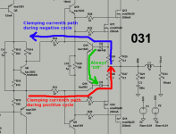
I might be wrong and I don't have access to any simulator to check it, but here's how I see it, the protection circuit for the output FET stage doesn't work as one might think, those 2 transistors Q15, Q16, and 2 diodes D3, D4, supposed to sense the voltage fall over the source resistors at 0,1 Ohm in the occurrence of a short at the output do nothing, or, almost nothing, because as we will soon see they do "protect" but in a peculiar way.
The lower side of the Vbe multiplier circuit, which is biasing the output stage, is during positive cycle clamped to the output through lower over current protection transistors collector-base diode + lower diode + source-R (Q16 + D4 + R26).
And vice-verse during negative output voltage cycle, the higher side of the Vbe multiplier circuit is clamped to the output through the upper transistors collector-base diode + upper diode + source-R (Q15 + D3 + R24), hence these two transistors do not act on the voltage fall over output FET source resistors more than two passive diodes via their base-collector diode.
And the reason the output clips harder for positive cycle is because the N-ch FET's have lower Vgs threshold than P-ch FET's, in any case the Vgs drive is always so low due to the clamping that the output FET's becomes self limiting without any protection circuit.
To make the output protection circuit (consisting of Q15, Q16, D3 and D4) engage during a short, we would need at the very least some 0,6 Volt voltage fall for each of ALL 4 devices (Q15, Q16, D3 and D4), ie. 2,4 Volt, and 2,4V over R24 alone equals to 24 Ampere for one output device, which doesn't happen due to the clamping effect explained above, ie. the protection circuit doesn't work as expected.
Attachments
Last edited:

petr_2009
All your posts that are unrelated to this thread have been split off to here:
Musings on amp design... a thread split.
If you wish a different title then please report post #1 of the new thread and say what you want it to be called.
Please in future do not hijack and drag other established threads off topic as you have this one.
SSassen, can you draw a rough sketch block diagram of your final 'balanced mode' application? I'm busy with a balanced bridge Hiraga with an unbalanced input, hence this question.Thanks! But these simulations fall apart when I run the amplifier in balanced mode, which really is a requirement for me.
ps:
Good split Mooly!
SSassen, can you draw a rough sketch block diagram of your final 'balanced mode' application? I'm busy with a balanced bridge Hiraga with an unbalanced input, hence this question.
Apologies for the late reply, work caught up with me
...Not entirely sure what you mean, the schematic as posted shows the balanced mode operation, which only applies to the input really, the output of the amplifier is single ended.
If you look at the amp as an operational differential amp, these things will matter imho. Resistor networks on inv and non-inv inputs should match precisely to yield max CMMRR - which translates to PSRR as well.
Yes, luckily we have commonly available 0.1% resistors that take will tackle this at reasonable cost.
I might be wrong and I don't have access to any simulator to check it, but here's how I see it, the protection circuit for the output FET stage doesn't work as one might think <snip>
petr_2009 was kind enough to simulate it here, so you won't have to take just my word for it, please see below quoted link.
Musings on amp design... a thread split.
Alright, on with the show! I was rummaging through my parts drawer and found some spare transistors, a few LEDs, some resistors and an inductor and figured I throw them in for good measure. We've dropped THD 20K at 100W in 8R down by another order of magnitude (0.000081%), but that's just in the simulator of course. Notable changes are:
1) L4 a 10uH inductor that helps to up the loop gain at lower frequencies.
2) Q27 and Q28 to make the input a complimentary feedback pair (Sziklai).
3) Cascoded the current mirror for the input pair.
4) Cascoded the VAS/TIS section at the same time, a genuine two for one special!
5) Pick off points for the feedback network across the output resistors, hopefully dealing with rail distortion.
And yes, I know I'm suffering from feature creep, I keep telling myself that a few more transistors won't break the bank, and they won't, and I know I'm straying from the path of KISS again, you guys better reel me in before I go off the deep end again!
Attachments
Does 2) improve anything in simulation?Alright, on with the show! I was rummaging through my parts drawer and found some spare transistors, a few LEDs, some resistors and an inductor and figured I throw them in for good measure. We've dropped THD 20K at 100W in 8R down by another order of magnitude (0.000081%), but that's just in the simulator of course. Notable changes are:
1) L4 a 10uH inductor that helps to up the loop gain at lower frequencies.
2) Q27 and Q28 to make the input a complimentary feedback pair (Sziklai).
3) Cascoded the current mirror for the input pair.
4) Cascoded the VAS/TIS section at the same time, a genuine two for one special!
5) Pick off points for the feedback network across the output resistors, hopefully dealing with rail distortion.
And yes, I know I'm suffering from feature creep, I keep telling myself that a few more transistors won't break the bank, and they won't, and I know I'm straying from the path of KISS again, you guys better reel me in before I go off the deep end again!
By itself not much, it needs the added cascode for the current mirror.Does 2) improve anything in simulation?
I see a boucherot 100n/4R7Outstanding simulation...
You are using unusually low gate stoppers in the output laterals..... Are you planning some special arrangement to avoid oscillations ?
Outstanding simulation...
You are using unusually low gate stoppers in the output laterals..... Are you planning some special arrangement to avoid oscillations ?
Yes and no, just good local decoupling and tweaking the gate stoppers on the prototype.
Same here, but..In my builds I got good results with 270ohm for 20N20 and 180 for 20P20.
I also added 15p between each gate and drain.
And 15n decoupling very close to each drain.
Never seen such low 20THD sim......
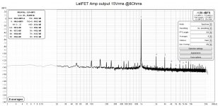
my REW measurements came out better than the sim
Attachments
Nice results! What did you use to make these measurements?Same here, but..
my REW measurements came out better than the sim
I needed a better soundcard, and the Motu M4 did the trick for an affordable price. It is a pity that the full resolution line input only works with windows - arghhhNice results! What did you use to make these measurements?
- Home
- Amplifiers
- Solid State
- Simplicity and elegance, feedback wanted!