Hello all,
Wondering if anyone has done tests to optimize the value of current compensation resistor (R39 on the attached schematic) to minimize the shift in amplifier bias setting with changes in the +B supply rail voltage. If so, what results were obtained.
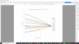
I just ran a real world test on various values of resistor ( 0 to 91ohms) and found the optimal value to be 36ohms, which is much higher than the conventionally suggested value of about 13ohms for the 10mA VAS current being used. Interestingly this agrees with the optimal value which my LTSpice simulations predicted while designing the amplifier. At that time I suspected my SPICE simulation was erroneous since it did not agree with what I read in certain books on amplifiers.
Wondering if anyone has done tests to optimize the value of current compensation resistor (R39 on the attached schematic) to minimize the shift in amplifier bias setting with changes in the +B supply rail voltage. If so, what results were obtained.
I just ran a real world test on various values of resistor ( 0 to 91ohms) and found the optimal value to be 36ohms, which is much higher than the conventionally suggested value of about 13ohms for the 10mA VAS current being used. Interestingly this agrees with the optimal value which my LTSpice simulations predicted while designing the amplifier. At that time I suspected my SPICE simulation was erroneous since it did not agree with what I read in certain books on amplifiers.
Attachments
One thing to bear in mind is that you should not be trying to make a bias generator that does not alter its voltage with current.
What is needed is a bias generator which when combined with the output stage, gives minimal variation in the output stage quiescent current when the supply voltage varies.
It is a different target.
What is needed is a bias generator which when combined with the output stage, gives minimal variation in the output stage quiescent current when the supply voltage varies.
It is a different target.
One thing to bear in mind is that you should not be trying to make a bias generator that does not alter its voltage with current.
What is needed is a bias generator which when combined with the output stage, gives minimal variation in the output stage quiescent current when the supply voltage varies.
It is a different target.
I did read your elaboration on that point last night (Self on Amplifiers v.6) and it sounds like it is not a simple matter to perform this optimization given the shifting points of driver/output devices with temperature variations. I will have to re-read that section again (slowly) and plan how to proceed.
I assume with these kind of bias circuits that the dc current flowing through it is constant when no ac signal is applied to the input (or this Hawksford - Early effect would kick in; ref #5).
So the optimum value for the bias compensation is different from the power supply compensition value. These are different phenomena and one resistor cannot perform two duties at the same time. But it is very interesting indeed.
How is the current through the bias circuit made?
With an input differential and a accurate current source (ps independent), and a current mirror vas setup, one might expect a ps independent current running through the bias circuit. If it is not a current source but only a simple resistor, the current will drift with the ps. If no mirror is used but only a resistor, this current will drift too. With both resistors used, more drift will happen. A small drift in the first stage will be amplified in the second, the high gain vas.
Can you show the rest of the circuit? By exchanging parts or segments of the complete circuit it could show less dependency of ps variation. The ideal would be to find the proper topology where R39 can remain the same 13Ω.
And measure it after building it of course to verify the simulations!
The only sure way is to build it and measure it.
SPICE representation of Early effect (which is at the heart of this) is rudimentary.
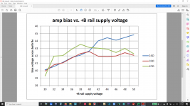
Thank you Douglas for your reply. I have done just that with three values of resistor (16, 33 and 47 ohms) on a build of my current amplifier board and found the results to be pleasantly in line with what I observed in SPICE calculations and with a breadboard buildup of the VBE multiplier subcircuit alone.
For my particular amplifier the optimal value for this resistor (R39 on my schematic) appears to be about 36ohms in all three cases. (I did not have a 36ohm resistor handy today). I apologize for the roughness of the data points in today's graph. They are actual measurements using the averaging function in my HP34401A DMM. (Please note the bias voltage levels (Y-axis) are in mV)
I think perhaps the simple calculation sometimes used of R = intrinsic emitter resistance (re) * VBE multiplication factor (4 in my case for two stage EF output) needs to be re-thought. I believe Douglas may have elaborated on this in a section is his tour-de-force on audio amplifiers Ver.6. I will have to re-read this material tonight and see if this is the case.
For now I will be moving back to determining optimal values for components integral to compensation. First the lowest value of Miller compensation capacitor consistent with stable operation, then optimal values for C1, C2 and R in order to jumper over to TMC (output inclusive) compensation.
(PS I have no idea why my 2nd image keeps showing up upside down! )
Attachments
Can you show the rest of the circuit? By exchanging parts or segments of the complete circuit it could show less dependency of ps variation. The ideal would be to find the proper topology where R39 can remain the same 13Ω.
And measure it after building it of course to verify the simulations!
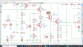
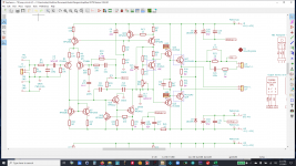
Thanks for the input. I have attached a picture of the whole schematic for one channel
Attachments
Thank you Douglas for your reply. I have done just that with three values of resistor (16, 33 and 47 ohms) on a build of my current amplifier board and found the results to be pleasantly in line with what I observed in SPICE calculations and with a breadboard buildup of the VBE multiplier subcircuit alone.
)
I hope you realise I meant build the Vbe generator AND the output stage.
Yes Douglas. I did understand your reply and my tests today were on a complete amplifier channel. I found it interesting that my measurements agreed with the same findings that SPICE simulation and breadboarding just the VBE multiplier & VAS current source produced
(to close enough degree given I only used three resistor values on the actual board today due to the lack of resistor values on hand in the sub-50ohm range and the time involved modifying a PCB)
(to close enough degree given I only used three resistor values on the actual board today due to the lack of resistor values on hand in the sub-50ohm range and the time involved modifying a PCB)
Hi Mike,
I haven't really thought that much about supply independent bias current for the output drivers, but I like your approach.
In a standard amp, the supply is more or less constant, so I haven't cared about this. In a class G or H system, however, I think this compensation is an important consideration. As Doug Self has noted the relative Early voltages of the Vbe multiplying transistor and the output transistors is what controls the compensating R value. These Early voltages tend to be highly variable in production, so each amplifier channel you build would have to be hand tweaked.
I just had another thought. When you vary the supply, you're also changing the temperature of the output transistors. The bias compensation should already be correcting for this, however.
In simulation, these factors are easy to separate, but on the bench it will be several seconds before the output bias current stabilizes after you change the rail voltage.
I haven't tried to simulate the thermal effectiveness of Vbe multipliers of discrete transistor amps using SPICE. I do not think the thermal Vbe models of some of the transistors are at all accurate. I understand some being -1.6mV/C, while others are -2.2mV/C. That's variation in geometry and doping. Some of my transistor models show -0.4mV/C, and I don't believe those models.
The current through the bias is set with the current source made of Q11 and Q19.Thanks for the input. I have attached a picture of the whole schematic for one channel
Take this section (Q11, R25, R27, R13, R37, Q19) in a separate simulation, give it a load of 4.2kΩ to the negative rail - the collector of Q19 will set around 0Vdc.
Then vary the rails to determine the ps dependency of this current source.
Curious to view the graph.
(I've no time now to simulate it myself and your models are unknown.)
Also, the input diff cs is also depending on these results.
Hi Mike,
I haven't really thought that much about supply independent bias current for the output drivers, but I like your approach.
In a standard amp, the supply is more or less constant, so I haven't cared about this.
Actually the conventionally unregulated amp supply voltages do vary quite a bit due to the effects of amplifier loading and AC power line variance geographically, seasonally, daily, etc.
My next amp (for various reasons) I do plan on using separate, regulated supplies for the amp front end (VAS & IPS). With a single dual (+/-) amp supply obviously regulating the IPS & VAS section rails produces problems with restricted clipping headroom due to regulator voltage drop. But I digress...
From what I have seen a careful optimization of the current compensation resistor on the VBE transistor collector can very much reduce +B rail variance induced shifts in bias adjustment. I'm not sure if the value can be calculated or must be selected by tuning a finished amplifier design. The calculation I have seen suggested is not correct it appears. And there may be other ways (as suggested) of producing bias adjustment than the conventional VBE multiplier. But I had already designed this amplifier using a VBE multiplier and am now in the optimization phase on Version 3.0, which I expect is the last for this amplifier.
The current through the bias is set with the current source made of Q11 and Q19.
Take this section (Q11, R25, R27, R13, R37, Q19) in a separate simulation, give it a load of 4.2kΩ to the negative rail - the collector of Q19 will set around 0Vdc.
Then vary the rails to determine the ps dependency of this current source.
Curious to view the graph.
(I've no time now to simulate it myself and your models are unknown.)
Also, the input diff cs is also depending on these results.
I believe the root of the problem is the sensitivity of the VAS current source to supply voltage variation. It is not a perfect current source. This issue is well known and the resistor R39 is supposed to compensate for it. My problem was accurately determining this resisitor value as the "textbook" method I had been using was just wrong.
I just had another thought. When you vary the supply, you're also changing the temperature of the output transistors. The bias compensation should already be correcting for this, however.
In simulation, these factors are easy to separate, but on the bench it will be several seconds before the output bias current stabilizes after you change the rail voltage.
I haven't tried to simulate the thermal effectiveness of Vbe multipliers of discrete transistor amps using SPICE. I do not think the thermal Vbe models of some of the transistors are at all accurate. I understand some being -1.6mV/C, while others are -2.2mV/C. That's variation in geometry and doping. Some of my transistor models show -0.4mV/C, and I don't believe those models.
Yes, that had occurred to me also. I'm not really sure an optimal bias setting for a class B (or AB depending on your religion) amplifier is obtainable in the real world while music is playing, producing shifts in device temperatures and supply voltage variations of wildly varying time delays. (This type of thing is one of the reason Douglas's book is so darn long - he explores many of these issues)
For this reason I am considering using a displaced crossover design on my next amplifier once I educate myself on it more. Both Bob and Douglas have written on this architecture I believe. At this point I am only versed in the general theory, not the nuts and bolts of design.
From what I have seen a careful optimization of the current compensation resistor on the VBE transistor collector can very much reduce +B rail variance induced shifts in bias adjustment.
Just use a CFP-based bias generator and you won't have to worry about all this stuff.
- Status
- This old topic is closed. If you want to reopen this topic, contact a moderator using the "Report Post" button.
- Home
- Amplifiers
- Solid State
- VBE Multiplier current compensation resistor