That is a very interesting observation. I have used MJE340/50 transistors for drivers and the VBE transistor for several reasons, but I will definitely look into speed of response when I begin designing my next amplifier and consider using a transistor with a lower VCEO, presumably a smaller die size.
I think the rate of change of temperature of the surface that the VBE transistor is mounted to MAY make this a moot point, but it is certainly worth looking into.
On my latest amplifier, finished this week, the output transistors are TO-3 devices. I mounted the VBE transistor to the top of one of the TO-3 devices, and it certainly allows much faster thermal tracking by the bias control circuitry than mounting it on the heatsink. I also tested mounting the bias transistor on the TO-3 device flange, but that was also much slower than attaching it to the top of the TO-3 transistor.
I don't think thermal inertia and die size play a role in that: the total volume of the package (TO126 for example) remains identical, and there are no substantial, decisive differences in the volumic heat capacity of the various solid materials (metal, silicon, epoxy); in fact, epoxy might well have a higher capacity due to phase transitions.
Transistors having a low Vceo are probably correlated to a higher Is, meaning a higher tempco for a given current, resulting in a higher sensitivity (just a hypothesis)
Transistors having a low Vceo are probably correlated to a higher Is, meaning a higher tempco for a given current, resulting in a higher sensitivity (just a hypothesis)
Just for the fun of it, I was wondering how these kind of amplifiers behave in my Spice environment (AimSpice by Trond Ytterdal) and with my standard selection of simulations (DC, PSRR, open loop, closed loop with tweakings). Transients and other distortion drilling I leave to others.... I'd have to simulate it in Spice...
The models are kept as simple as possible (only beta defined), so one sees the amp doing things to compensate for what the bjt's are doing wrong, and more.
I followed the nodes-numbering as close as possible to the parts numbers. Exceptions are node 57 (base Q15), 50 (collector Q17), 52 (collector Q19), 60 (pre zobel) and 66 (post zobel). These are the stepstone nodes in the amplifier to understand it's inner behaviour. Just a musing: is it wise to connect the feedback post zobel? It puts an extra task on the feedback (read amplifer) to adjust for extreme frequencies.
Discontinuities in the phase plots are normal jumps in the scaling.
The dc jump at startup is over 0.6Vdc, which is allowable, but a relay prevents nasty things (see above the feedback post zobel connecton!).
The dc jump at 'stopend' is caused by an uncontrolled anymore Q19 (node 52).
Both jumps are due to the failing feedback when the supplies are under 4 or 2 Vdc (symmetric rise/fall assumed), so quite swift though to prevent for further derailments. (Notice 'stopend' reads right to left due to simu constraints; I'm running it on W2k in a VMware sandbox.)
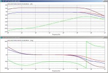
Ripple is injected symmetrically with a 1Vac source on the supplies for calculation convenience (PSRR wih ref to 1Vac).
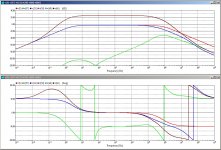
Open loop is done with an input of 0.0775Vac = -40dB, same reason.
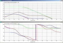
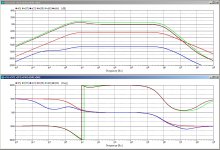
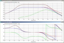
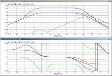
Bode- and compensation plots all in the same scaling - boy oh boy, what a horrible phase response - as a compensation of the semiconductor potpourri. Definitly not my suit. But fun anyhow.
Attachments
-
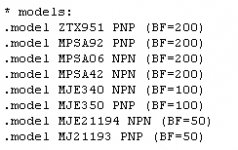 01_MikeyAmp_models.jpg16.5 KB · Views: 141
 -
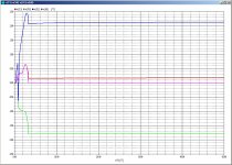 02_MikeyAmp_DCstartup.jpg428.5 KB · Views: 141
 -
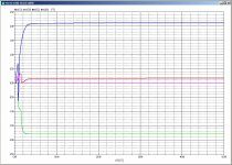 03_MikeyAmp_DCstopend-inverse.jpg431.1 KB · Views: 134
 -
 04_MikeyAmp_PSRR-1Vripple.jpg353.4 KB · Views: 129
 -
 05_MikeyAmp_AC-Openloop-77.5mV.jpg358.8 KB · Views: 130
 -
 06_MikeyAmp_AC-Bode.jpg328.6 KB · Views: 61
 -
 07_MikeyAmp_AC-Bode-C17.jpg364.8 KB · Views: 60
 -
 08_MikeyAmp_AC-Bode-R29.jpg366.2 KB · Views: 64
 -
 09_MikeyAmp_AC-Bode-C17-R29.jpg369.2 KB · Views: 65
Hello MarsBravo,
Very interesting SPICE simulations. I did ponder over where to place locate the node for output feedback to the TMC resistor. I decided to place it after the Zobel network in order to enclose within the feedback loop the entire output stage right to the output connector. This was a gamble, but I could find no articles that shed light on the matter beforehand.
I can attest that it certainly appears stable under normal operation (playing music via conventional two-way speakers), into 4ohm dummy loads, and when driven by square waves.
I will have to measure the DC startup voltage spike out of curiosity. I do know that it settles to > 5mV quite quickly on startup with 40V rails.
I did notice that clipping into heavy loads on the negative going sine peak did have some unattractive ringing. There may be a problem there which could preclude it from reliable use as a commercial product, didn't pursue it. I did not take time in the design phase to manage clipping in a controlled fashion (VAS clipping with respect to output stage clipping) as this is for my own personal use in my vintage Pioneer SX-750 receiver and not as a saleable product.
Welcome any feedback and thanks, Mike
- Status
- This old topic is closed. If you want to reopen this topic, contact a moderator using the "Report Post" button.