
I see no reason why you should damage anything, but it’s a very complex amplifier and I think it’s therefore better not to try.
Also because your power regulator is so simple that it can’t be too difficult to find the cause with the help of Mooly.
Hans
Hi Hans, thx for your feedback.
While waiting for components, I reviewed again the whole circuit.... no problem found.
But must be somewhere....!
There is a strange circuit with optocoupler, which goes nowhere... I will focus on this tomorrow...
Unfortunately I do not have all schematics... still trying to find them...
Theodore
Theodore,
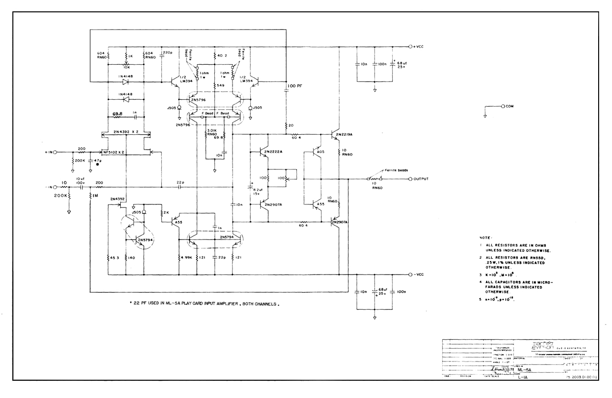
This is all 100% ML family structure, going back to ML27.5, the ML23.5 and the ML20.6.
At the left you see exactly the start up circuit with Fet and two bipolars that I described at the start of your thread.
Next to is is the output current protection and then comes the overvoltage protection.
Also the end stage or current amplifier is spot on Mark Levinson.
Hans
What I still forgot is the DC output voltage sense and the heat sensor circuit at the bottom that goes to an opto-coupler that will switch the amp off when exceeding the limits.
Last edited:
Hi Theo,
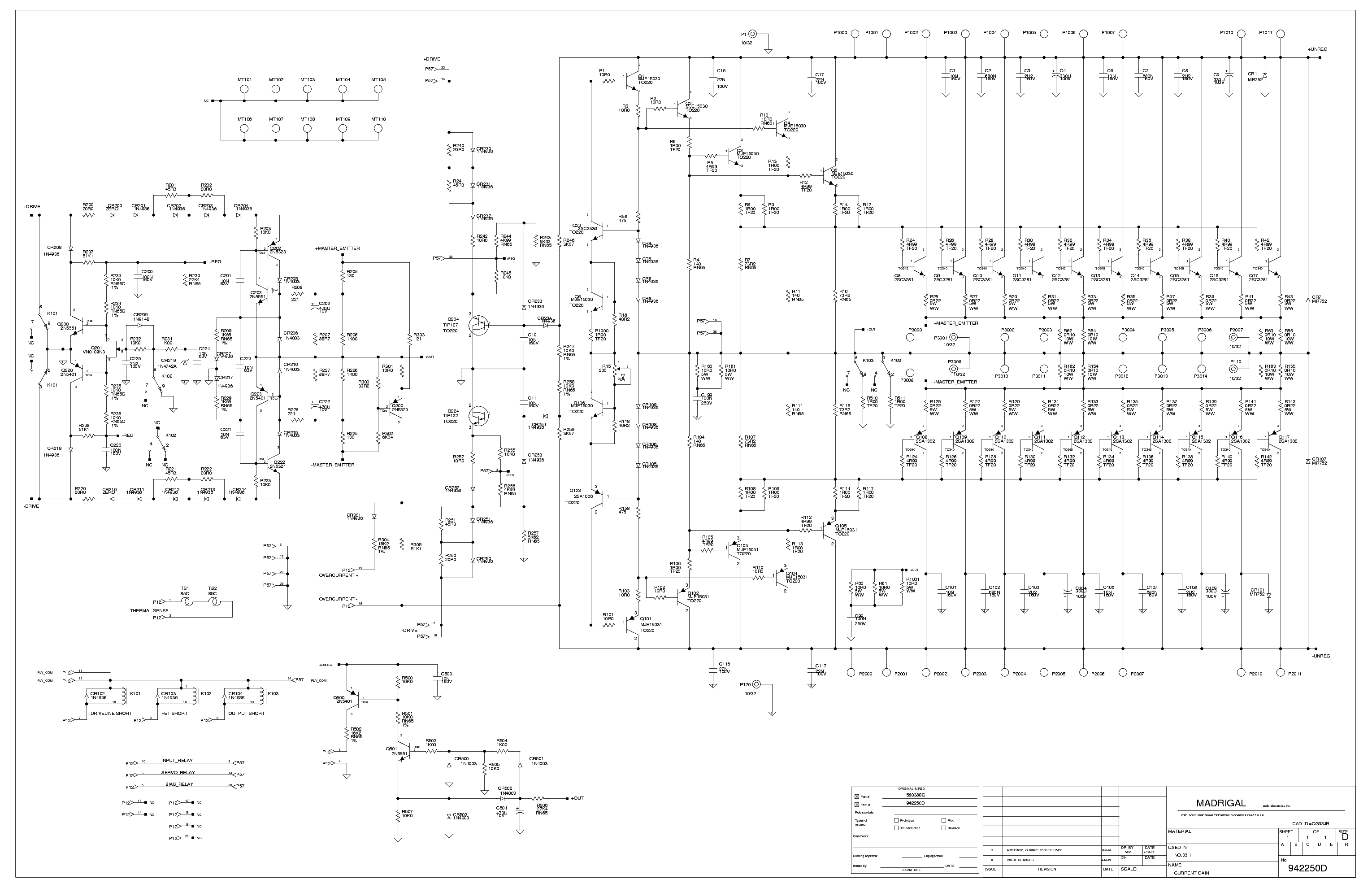
TRIP could be pulled up or pulled down, but only when R2 and R3 where installed AND when some signals were offered to the input of the 4N33's which in your drawing is not the case.
Maybe this was a leftover of previous models, where this function is now being taken over by software in the analogue processor.
But nevertheless strange that they haven't installed two low cost resistors but have left the more costly opto couplers.
Is this PCB a two layer board or could it be a multilayer board where signals are routed on the inner layers ?
You have drawn a short circuit between the inputs, was this really zero ohm, or could it be a bit more, indicating that something is still in between ?
Hans
Hi Hans,
yes it is strange!
But the other channel is exactly the same.
It seems that something went not as expected during tests and they did a last minute modification. Or this circuit is in use in ML336 ( i will check it when i manage to finally unpack my new purchase!!") )
)
The shorted pins (1,2) of optotransistors are soldered together. Normally this circuit looks like it goes instead of CR200 and CR210 of the ML 33H diagram (cast sent).
It is a dual layer PCB, at least the part i inspected. Maybe multilayer elsewhere but i don't think so.
Theodore
yes it is strange!
But the other channel is exactly the same.
It seems that something went not as expected during tests and they did a last minute modification. Or this circuit is in use in ML336 ( i will check it when i manage to finally unpack my new purchase!!
)The shorted pins (1,2) of optotransistors are soldered together. Normally this circuit looks like it goes instead of CR200 and CR210 of the ML 33H diagram (cast sent).
It is a dual layer PCB, at least the part i inspected. Maybe multilayer elsewhere but i don't think so.
Theodore
Theo,
You have drawn a 45K resistor from -Vreg to the opto coupler.
This can never take more than 2.5mA to gnd, the voltage regulator won’t even notice this.
Your regulator has no current limit provision, so if more current has to be supplied as envisaged, it will simply go on suppying -115 Volt up to a point where the MJE15031 finally breaks down.
But you have even replaced the MJE that was still intact, so whatever the opto coupler is doing, it can never let your voltage regulator derail by just nipping at it’s output.
Hans
Hans, Mooly,
I am (extremely) glad to inform you that today i received the spare parts (finally) and the problem found and solved!!!!!!
Thank you all very much for all your efforts!!!
For the records, the problem was the Q124, which was measured OK on board, but it was not working correctly.
However, this transistor gets extremely warm and i'm not sure if it will last... The relative on the other side (Q109) is also warm but not that much.
Any idea what could i do?
Theodore
Well that is good news, I'm pleased it all got there in the end.
Q124 wasn't my first suspect but it did crop up as a possible cause...
As I often say, fault finding is always about gathering evidence to piece together what has happened.
Well done
Q124 wasn't my first suspect
but it did crop up as a possible cause...Check that Q124 and Q125 are OK. There should be approx 1.1 to 1.2 volts across R163. These two transistors form a current source and if the current is low then you would get to little output volts.
As I often say, fault finding is always about gathering evidence to piece together what has happened.
Well done
And you say it gets hot... well I think it will because with around 22 milliamps flowing through it (and we know that because the B-E junction of the Darlington will see around 1.1 to 1.2 volts across it and that is across the 49.9 ohm resistor) and the fact the transistor has around 25 volts across it gives a dissipation of 550mw which is very close to the devices maximum of 625mw.
It might be worth replacing the opposite positive reg side (2N5551) as that will be similar.
You can (or could) get clip on heatsinks for TO92 packages.
It might be worth replacing the opposite positive reg side (2N5551) as that will be similar.
You can (or could) get clip on heatsinks for TO92 packages.
Congratulations and exactly what I expected after you measured only 80mV on R156 and R158 instead of 550mV as mentioned in posting #80.Hans, Mooly,
I am (extremely) glad to inform you that today i received the spare parts (finally) and the problem found and solved!!!!!!
Thank you all very much for all your efforts!!!
For the records, the problem was the Q124, which was measured OK on board, but it was not working correctly.
However, this transistor gets extremely warm and i'm not sure if it will last... The relative on the other side (Q109) is also warm but not that much.
Any idea what could i do?
Theodore
And yes, as Mooly mentioned it, 500mW is more than enough to make this transistor very hot.
Have lots of fun and hearing pleasure with your amps.
Hans
- Status
- This old topic is closed. If you want to reopen this topic, contact a moderator using the "Report Post" button.
- Home
- Amplifiers
- Solid State
- Mark Levinson No 335 - NO Bias in one channel / NEED HELP