Re: Question about CFP
hi lumanauw - how about (re?)reading the 1st few pages of this thread
you might find a good hint in higher bias for the drivers
the bd139/140 are not necessarily well behaved or fast when biased at <10 mA (through the 100 Ohm Rs) as in your schematic, why would you even consider controlling 10+ A output devices with a driver with so little bias?
As Eva commented there will be very poor turn off with so little current available - running the bd139/140 at 50 - 100 mA gets nearer their Ft peak and reduces excess feedback loop phase shift in addtion to speeding up turn off of the output Qs
after speeding up the feedback amplifer Qs with high bias you may not need to slow down the ouput devices so much - but only if your high frequency layout is really good
I reluctantly recommend the caps across the Rs at the output Q base-emitter junctions to slow down the output Qs and define a dominant pole - other compensation approaches don't account for real world psrr complications which are better avoided
Assuming a gain of 100 for all devices:
BD139/140 has an FT of approx 100Mhz so it introduces a pole at approx. 1Mhz and a zero somewhere below 100Mhz.
TIP35C/36C has an FT of approx 3Mhz so it introduces a pole at approx. 30Khz and a zero somewhere below 3Mhz.
When you add up both responses, you get almost a constant 6dB/oct rolloff with a phase shift that never reaches 180 degrees at any frequency where the system still exhibits feedback.
However, a 30Mhz output device with a gain of 100 introduces a pole at approx. 300Khz and a zero somewhere below 30Mhz, so in the frequency range comprised between 1Mhz and 30Mhz open loop phase shift may approach or exceed 180 degrees, thus leading to instability.
In order to solve that potential oscillation issue, I would use resistors to force the gain of the drivers to a lower value thus shifting their poles upwards, and B-C capacitors in the output devices to shift their poles downwards. The CFP should be stable when pole overlapping zone is made narrow enough to provide adequate phase margin.
There are other aspects of the circuit that may lead to instability, like B-E discharge resistors of the output devices that should be of a low enough value, improper supply decoupling or the lack of a proper resistive load in the output at high frequencies (the classic RC netword solves that).
Hi, Everyone,
I want to write about my experiment.
The output that I tried is 3 types, TIP35C-36C, C2922-A1216, C5200-A1943.
With TIP35C-36C, the whole amp is normal, stable.
I tried various capacitor (up to 100nF) in different places. In some places, the oscilation become worse.
Between B-C/driver, B-E/driver, C-E/driver, accross 10ohm, accross 100ohm, B-C/output, B-E/output, C-E/output, bridging between B-B/output.
Bridging from B-B of the output transistor seems not help (sorry, Bocka). Only in 2 places seems help, that is between B-C/driver or accross 100ohm (=B-E/output). BUT these 2 nees value up to 100nF, makes the trebles disappears.
For C2922-A1216 (which oscilate less than C5200-A1943), for unknown reason this helps. That is to change the VBE multiplier resistors. The VAS I use is biased at 7mA. In the original design I use 6k8-4k7, that works fine for TIP35C-36C, but makes oscilation for C2922-A1216 (and becomes oscilator for C5200-A1943).
I change the value to 3k-2k2, this helps for C2922-A1216, but still dont work for C5200-A1943.
The question is, if the problem is in the CFP, why changing the bias resistors can help? What is happening here?
And C5200 has ft about 30mhz, and C2922 has ft about 50mhz (from datahseet), but why C2922 oscilate less?
Hi, EVA,
What are the values do you suggest? And for not mistaken your advice, could you hand-draw your suggestion?
I want to write about my experiment.
The output that I tried is 3 types, TIP35C-36C, C2922-A1216, C5200-A1943.
With TIP35C-36C, the whole amp is normal, stable.
I tried various capacitor (up to 100nF) in different places. In some places, the oscilation become worse.
Between B-C/driver, B-E/driver, C-E/driver, accross 10ohm, accross 100ohm, B-C/output, B-E/output, C-E/output, bridging between B-B/output.
Bridging from B-B of the output transistor seems not help (sorry, Bocka). Only in 2 places seems help, that is between B-C/driver or accross 100ohm (=B-E/output). BUT these 2 nees value up to 100nF, makes the trebles disappears.
For C2922-A1216 (which oscilate less than C5200-A1943), for unknown reason this helps. That is to change the VBE multiplier resistors. The VAS I use is biased at 7mA. In the original design I use 6k8-4k7, that works fine for TIP35C-36C, but makes oscilation for C2922-A1216 (and becomes oscilator for C5200-A1943).
I change the value to 3k-2k2, this helps for C2922-A1216, but still dont work for C5200-A1943.
The question is, if the problem is in the CFP, why changing the bias resistors can help? What is happening here?
And C5200 has ft about 30mhz, and C2922 has ft about 50mhz (from datahseet), but why C2922 oscilate less?
Hi, EVA,
In order to solve that potential oscillation issue, I would use resistors to force the gain of the drivers to a lower value thus shifting their poles upwards, and B-C capacitors in the output devices to shift their poles downwards. The CFP should be stable when pole overlapping zone is made narrow enough to provide adequate phase margin.
What are the values do you suggest? And for not mistaken your advice, could you hand-draw your suggestion?
Attachments
Lumanauw,
I would get rid of those 10 R emitter resistors and connect the driver emitter directly to collcetor of output, and from there use a Emitter(Collector resistor) like 0,10-0,47 Ohm or so to output node.
I also agree with Bocka, to isolate "another" potential problem use a small cap from VAS to the feedback node.
And just a last note as you have not shown any pictures or talked about how the physical layout look like, I would strongly recommend you to put driver and output transistor and surrounding components belonging to the CFP circuit VERY CLOSE to each other, this is really important!
Then start again with a small capacitor between C and B of driver transistor, start with some 10 pF but do not exceed much more than 1nF or so, because if it goes much beyond 1nF I dont think it's not adressing the right problem.
It would be good for us also to know how your preceeding stage look like driving the CFP, so therefore above mentioned hints may not be valid!
Cheers Michael
Hi, Bocka and Michael,
Here's the pcb of the amp I talk about.
It is made by Protel 2.7, I hope you got it, because it cannot be opened by other program.
With this, you can look at the sch and also the placement I make.
http://valveaudio.tripod.com/diy/diydrive.pcb
http://valveaudio.tripod.com/diy/diymain.pcb
http://valveaudio.tripod.com/diy/diypwm.pcb
lumanauw said:Hi, Bocka and Michael,
Here's the pcb of the amp I talk about.
It is made by Protel 2.7, I hope you got it, because it cannot be opened by other program.
With this, you can look at the sch and also the placement I make.
http://valveaudio.tripod.com/diy/diydrive.pcb
http://valveaudio.tripod.com/diy/diymain.pcb
http://valveaudio.tripod.com/diy/diypwm.pcb
Try to get JPG, PNG, GIF PDF, PS or something bit more common out of your layout prog.
") Hopefully it has some sort of export function or print option so that you could use virtual printer that prints to file as a PDF or PS.
Hopefully it has some sort of export function or print option so that you could use virtual printer that prints to file as a PDF or PS.Sorry, I don't realize that everybody use Protel
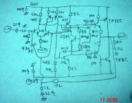
Here's the schematic, I just draw it 5 minute ago. Sorry about the quality, I got it with digital camera, not scanner.
I've used miller cap 100pf x 2, 27pf feedforward cap, it still oscilates (not with TIP35C-36C).
Maybe some of you will notice the strange part in the current mirror, I use very big 2k2. First it was 470ohm, but putting 2k2 there seems help.
Attachments
If I can help you with your CFP amp. I like your current mirror and symetrical design.
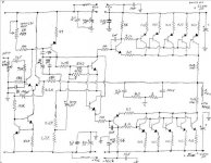
I built a CFP output amp, and it's stable. It was designed for subwoofer, but in testing it plays all frequencies clearly.
Has 5 pairs of MJL4281 MJL4302 output transistors, with MJE15034/35 drivers.
I had to take some extra steps for stability, because when first built, it oscillated. Now it runs fine. The schematic shows these changes that removed the oscillation.
Added 1nf caps for B-E of drivers, and 100ohm base resistors for drivers. The 100ohm+1nf is to filter RF.
I added 4.7 ohm emitter resistors for drivers for some degenerative feedback.
Going to a 0.22uf zobel cap instead of traditional 0.1 got rid of all tapping sound, when I would touch speaker wires or heatsinks with my fingers. Also added extra 1ohm/10nf zobel to make up for long wires, and to add extra filtering.
Added 0.15 ohm output resistors (helped a ton with bias)
Added 0.27uf 250V ceramic caps to filter power supply rails and also 2KV 10nf caps from computer PSU to filter incoming DC to the capacitors.
BTW, good luck with your amp.
You may get some replies to go to EF instead of CFP but with some tweaking, it works great if you can stop it from oscillating, so keep on it! I think collector drive is stronger anyway, and I like the sound of CFP.
Attachments
Hi, EWorkshop1708,
Nice design you have. If there is "for subwoofer" and "for fullrange" design, I would choose #91 as subwoofer and #92 as full range. Because #91 will inherently have low DC offset, and with #92 I can tailor some "Niceness" (only if you want to).
The PCB that I built is not fixed pcb, the front end (Differential+VAS) is in small PCB/card, so I can try various topologies with the same main pcb.
For the output stage I choose CFP, because it is something with it's own local feedback+current drive mode, different from EF (although I'm confused now with it's oscilation ). It have big current supply capability, but not with the expense of raising RE drop or raising VBe value drop. This makes VBEmultiplier value is less disturbed from the turn-on-turn-off point of view.
I advoid using RE (like 0.15/10W in your #92), because although it will give better bias stability, it will boost the transistor turnon-turnoff characteristic, that's because I only use 1 pair for 1 amp, trying to not have parrarel. You can see speaker load can dip to 1 ohm or less (although only for u-second), that means the drop in this 0.15 will exceeded far from VBE multiplier value. The drop in this 0.15 will take more voltage drop than VBE multiplier preset value. The transistor will be hardly turn-on or turn-off, and this process will take time to settle (Like EVA said in the earlier page of this thread). I think this is also why some designs like Electrocompaniet also don't use this RE, unless we incorporated smart/sliding bias, or use many parrareled output devices (you used 5 parrarel, that's better in the view of transistor turnon-turnoff characteristic), because when sudden peak current, it is divided for 5 x 0.15ohm RE, making drop in each is less.
I've got a different card that is using the topology you have in #92. It is nice to use bootstrapped VAS, it gives more swing and more importantly it is giving very tight AC relationship between output node to VAS (due to bootstrapped capacitor), giving better audio phase response for the whole amp.
The difference in my card and your #92 is that for tail CCS I use 5k1 (like #91) supplied with carefully regulated -12V (opamp based regulator+capacitance multiplier to give very clean -12V).
Another difference is that the input and feedback Rdivider is symetrical (like #91) and I dont use LPF to ground (100pf in your #92), but using 470pf bridging from base of left to base to right (like #91). For me this method gives better result than making LPF towards ground, this 470pf will bypass any signal higher than its cut frequency not entering the differential system, and plus a bonus, this cap will again give better phase corelation between input and output node. This method is used by Electrocompaniet and suggested by JonathanCarr (well, that means it comes from 2 reputable sources).
In my card (that similiar to your #92), the OFFSET ADJ VR 680ohm is not used for adj offset, but it is used for "NICENESS KNOB". You can try this, adjust that 680VR until the DC offset is about 100mV (don't worry, I think it won't ruin your speaker), you will be able to hear "niceness sound" (with the expense of DC offset).
This "NICENESS" knob is trendy now, look at NP's PLH
Another difference is that the value of the VBE multiplier capacitance is only 10nF (like #91), and I try to flatten the OL response by adding 220kohm // with 100pf miller cap.
In my design #91, I try to flatten this OL gain by different approach, by putting IN4148 in the differential leg. This will reduce OL loop and extend OL bandwith.
But for subwoofer amp, maybe you can put only R for differential leg, cause subwoofer amp usually need high OL gain, not care about OL bandwith.
To give more tight relation ship and better input-output phase response, I add 4k7 resistors between VBE multiplier and output node before the base stoppers (Like Threshold statis 2-3). This also gives better audio result.
Nice design you have. If there is "for subwoofer" and "for fullrange" design, I would choose #91 as subwoofer and #92 as full range. Because #91 will inherently have low DC offset, and with #92 I can tailor some "Niceness" (only if you want to).
The PCB that I built is not fixed pcb, the front end (Differential+VAS) is in small PCB/card, so I can try various topologies with the same main pcb.
For the output stage I choose CFP, because it is something with it's own local feedback+current drive mode, different from EF (although I'm confused now with it's oscilation
). It have big current supply capability, but not with the expense of raising RE drop or raising VBe value drop. This makes VBEmultiplier value is less disturbed from the turn-on-turn-off point of view. I advoid using RE (like 0.15/10W in your #92), because although it will give better bias stability, it will boost the transistor turnon-turnoff characteristic, that's because I only use 1 pair for 1 amp, trying to not have parrarel. You can see speaker load can dip to 1 ohm or less (although only for u-second), that means the drop in this 0.15 will exceeded far from VBE multiplier value. The drop in this 0.15 will take more voltage drop than VBE multiplier preset value. The transistor will be hardly turn-on or turn-off, and this process will take time to settle (Like EVA said in the earlier page of this thread). I think this is also why some designs like Electrocompaniet also don't use this RE, unless we incorporated smart/sliding bias, or use many parrareled output devices (you used 5 parrarel, that's better in the view of transistor turnon-turnoff characteristic), because when sudden peak current, it is divided for 5 x 0.15ohm RE, making drop in each is less.
I've got a different card that is using the topology you have in #92. It is nice to use bootstrapped VAS, it gives more swing and more importantly it is giving very tight AC relationship between output node to VAS (due to bootstrapped capacitor), giving better audio phase response for the whole amp.
The difference in my card and your #92 is that for tail CCS I use 5k1 (like #91) supplied with carefully regulated -12V (opamp based regulator+capacitance multiplier to give very clean -12V).
Another difference is that the input and feedback Rdivider is symetrical (like #91) and I dont use LPF to ground (100pf in your #92), but using 470pf bridging from base of left to base to right (like #91). For me this method gives better result than making LPF towards ground, this 470pf will bypass any signal higher than its cut frequency not entering the differential system, and plus a bonus, this cap will again give better phase corelation between input and output node. This method is used by Electrocompaniet and suggested by JonathanCarr (well, that means it comes from 2 reputable sources).
In my card (that similiar to your #92), the OFFSET ADJ VR 680ohm is not used for adj offset, but it is used for "NICENESS KNOB"
. You can try this, adjust that 680VR until the DC offset is about 100mV (don't worry, I think it won't ruin your speaker), you will be able to hear "niceness sound" (with the expense of DC offset).This "NICENESS" knob is trendy now, look at NP's PLH
Another difference is that the value of the VBE multiplier capacitance is only 10nF (like #91), and I try to flatten the OL response by adding 220kohm // with 100pf miller cap.
In my design #91, I try to flatten this OL gain by different approach, by putting IN4148 in the differential leg. This will reduce OL loop and extend OL bandwith.
But for subwoofer amp, maybe you can put only R for differential leg, cause subwoofer amp usually need high OL gain, not care about OL bandwith.
To give more tight relation ship and better input-output phase response, I add 4k7 resistors between VBE multiplier and output node before the base stoppers (Like Threshold statis 2-3). This also gives better audio result.
Re: Speaking of Diamond buffers...
I do not know if I am late?
or did I brake the law?
but please look at simulated circuit.
Sorry for the mess, I was hurry:
The transistors of the first stage are BC546A/556A,
the second BD135/136
the third 2N3055/2955 (for the simulation purposes only).
Instead of ccs I used large resistors.
The circuit with an input 2V~ (straight from CD output) produces +- 6V~pp ath the output.
the second harmonic is at about -60dB
the third -40dB
rest at about -70dB, odd are higher.
Any sugestion or comments how to modify the values of the parts?
JonMarsh said:Speaking of diamond buffers, I'm surprised these guys haven't come up more around here in the discussions of unusual amplifiers... or even come up at all?
~JonAn externally hosted image should be here but it was not working when we last tested it.
I do not know if I am late?
or did I brake the law?
but please look at simulated circuit.
Sorry for the mess, I was hurry:
The transistors of the first stage are BC546A/556A,
the second BD135/136
the third 2N3055/2955 (for the simulation purposes only).
Instead of ccs I used large resistors.
The circuit with an input 2V~ (straight from CD output) produces +- 6V~pp ath the output.
the second harmonic is at about -60dB
the third -40dB
rest at about -70dB, odd are higher.
Any sugestion or comments how to modify the values of the parts?
Attachments
That cct is protected by patent #6,882,225.
From the manufacturer's website, I read something. That cct likely will have DC offset bias wandering from -0.6V to +0.6V (range =1V2).
What makes this "not stable" DC offset value? All openloop diamond buffer will act like this?
From the manufacturer's website, I read something. That cct likely will have DC offset bias wandering from -0.6V to +0.6V (range =1V2).
What makes this "not stable" DC offset value? All openloop diamond buffer will act like this?
- Status
- This old topic is closed. If you want to reopen this topic, contact a moderator using the "Report Post" button.
- Home
- Amplifiers
- Solid State
- Question(s) about CFP.