Hi there
I am trying to achieve a wide range (>100) tracking between two CCS's having a 1:100 ratio.
I need them for a beefed up version of this beta tester:
https://www.diyaudio.com/forums/equipment-and-tools/349199-constant-ic-tester-master.html
I want to build a 5mA to 5A version, but with the capability of reaching 50µA on the 5mA range.
For regular ranges, tracking in a 1 to 10 ratio is OK, but for the first range, a 1 to 100 ratio with an acceptable accuracy is required.
Because of the configuration (NPN/PNP), I want to keep things simple (no opamps).
This shows the basic option:
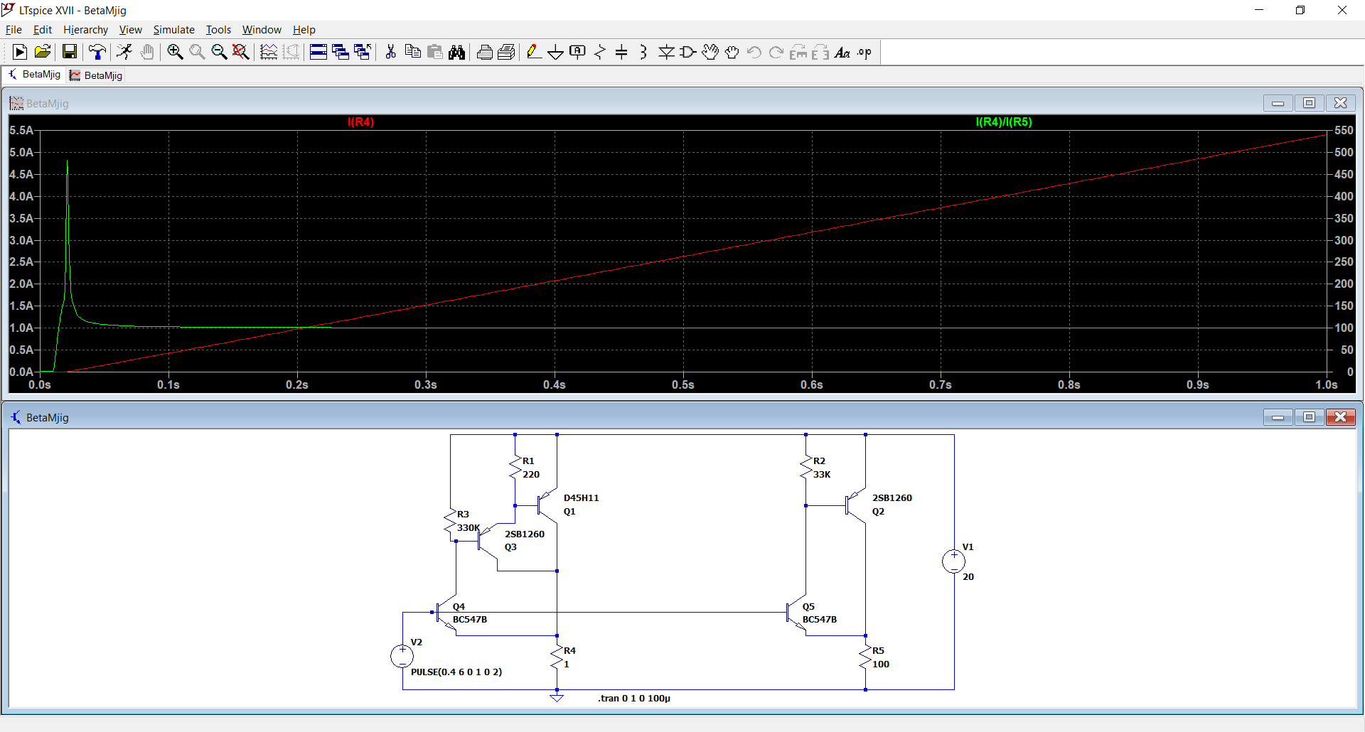
At low currents, there is a quirk;
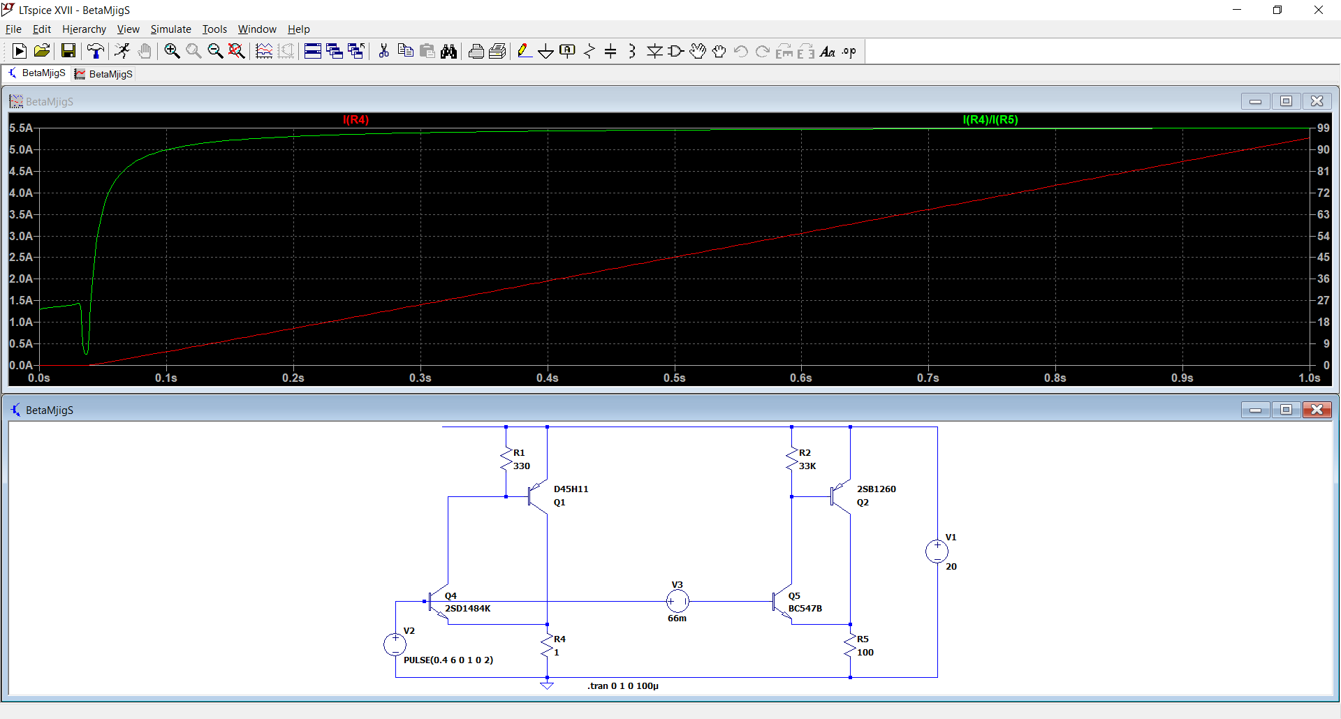
Another approach:
This one is a direct application of the basic theory, but it has other issues:
Etc, etc (I tried many other options)
Any ideas? (taking into account all the constraints, obviously)
I am trying to achieve a wide range (>100) tracking between two CCS's having a 1:100 ratio.
I need them for a beefed up version of this beta tester:
https://www.diyaudio.com/forums/equipment-and-tools/349199-constant-ic-tester-master.html
I want to build a 5mA to 5A version, but with the capability of reaching 50µA on the 5mA range.
For regular ranges, tracking in a 1 to 10 ratio is OK, but for the first range, a 1 to 100 ratio with an acceptable accuracy is required.
Because of the configuration (NPN/PNP), I want to keep things simple (no opamps).
This shows the basic option:
At low currents, there is a quirk;
Another approach:
This one is a direct application of the basic theory, but it has other issues:
Etc, etc (I tried many other options)
Any ideas? (taking into account all the constraints, obviously)
Attachments
My starting point would be to use 100 identical (closely matched, at least) devices to the reference device so that all Vbe's would be the same. Emitter resistors all the same. Currents nominally identical, but the 100 will give you a 100x gain.
Don't suppose that is what you had in mind, though. I have used this approach for a 10x gain successfully.
Next best, try equal Vbe's on small and large transistors and measure the currents. Then, depending on the ratio between them, say N, parallel 100/N devices for the 100x gain with the reference resistor R/N for each mirror emitter.
Difficulty is, as you indicate, is keeping everything balanced. This means keeping the collector voltages as equal as possible, and importantly the temperature.
Yes, the massively parallel approach would work much better than the solutions I tried, but it is a true brute force method, further complicated by the need to have the emitter resistors switched for the 4 ranges.
Having scaled transistors is the next best thing, but it will require quite a number of real measurements since spice is more or less useless in this case.
I had in mind a "smart" approach: for example servoing the voltage across the second emitter resistor to the first, using a 1 or 2 transistor pseudo-opamp, but it requires a bias supply beyond the rails which would seriously complicate matters, since presently the N/P selection is made by simply reversing the whole supply voltage.
And because the N and P circuits are simply paralleled, the "ghost" circuit of the opposite polarity must not disturb the active one.
BTW, in the last example I gave, V3 should be 120mV, not 60mV
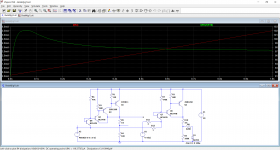
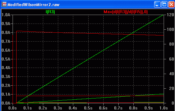
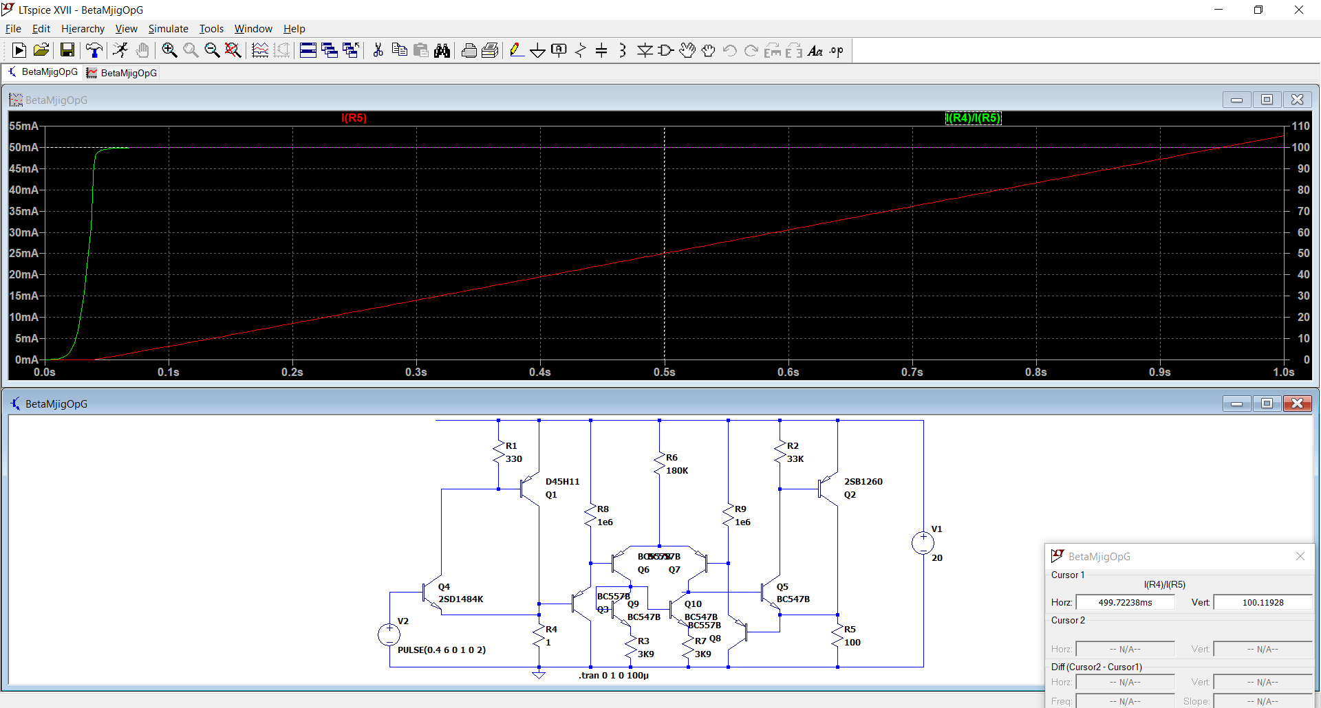
Here you are:
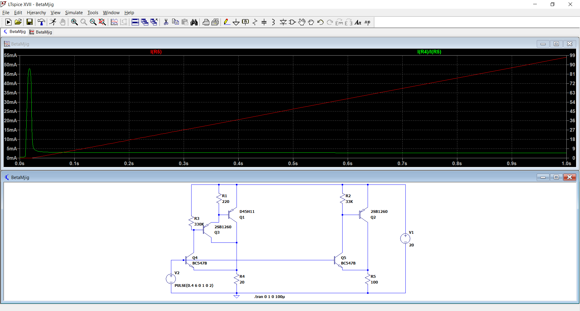
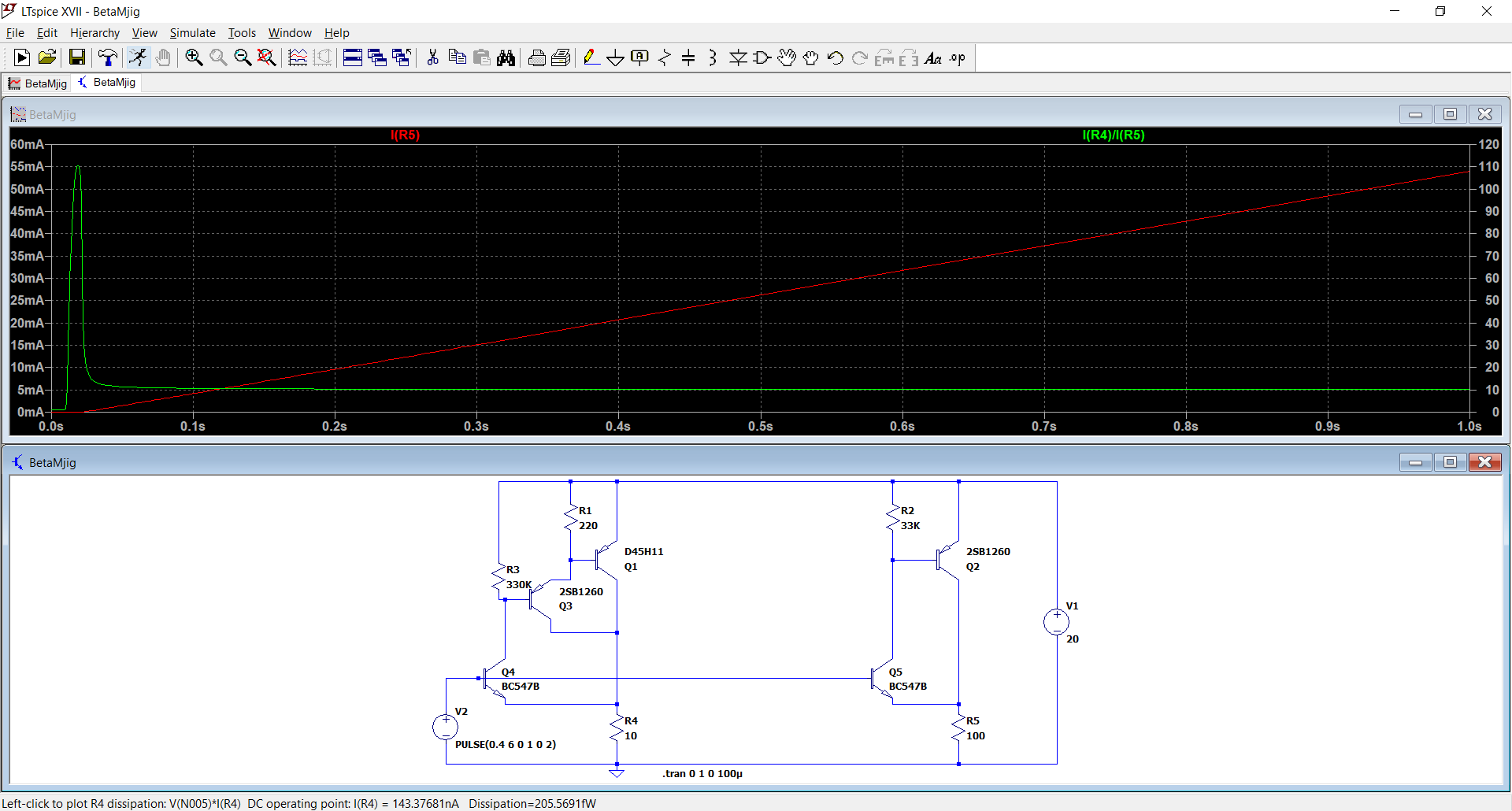
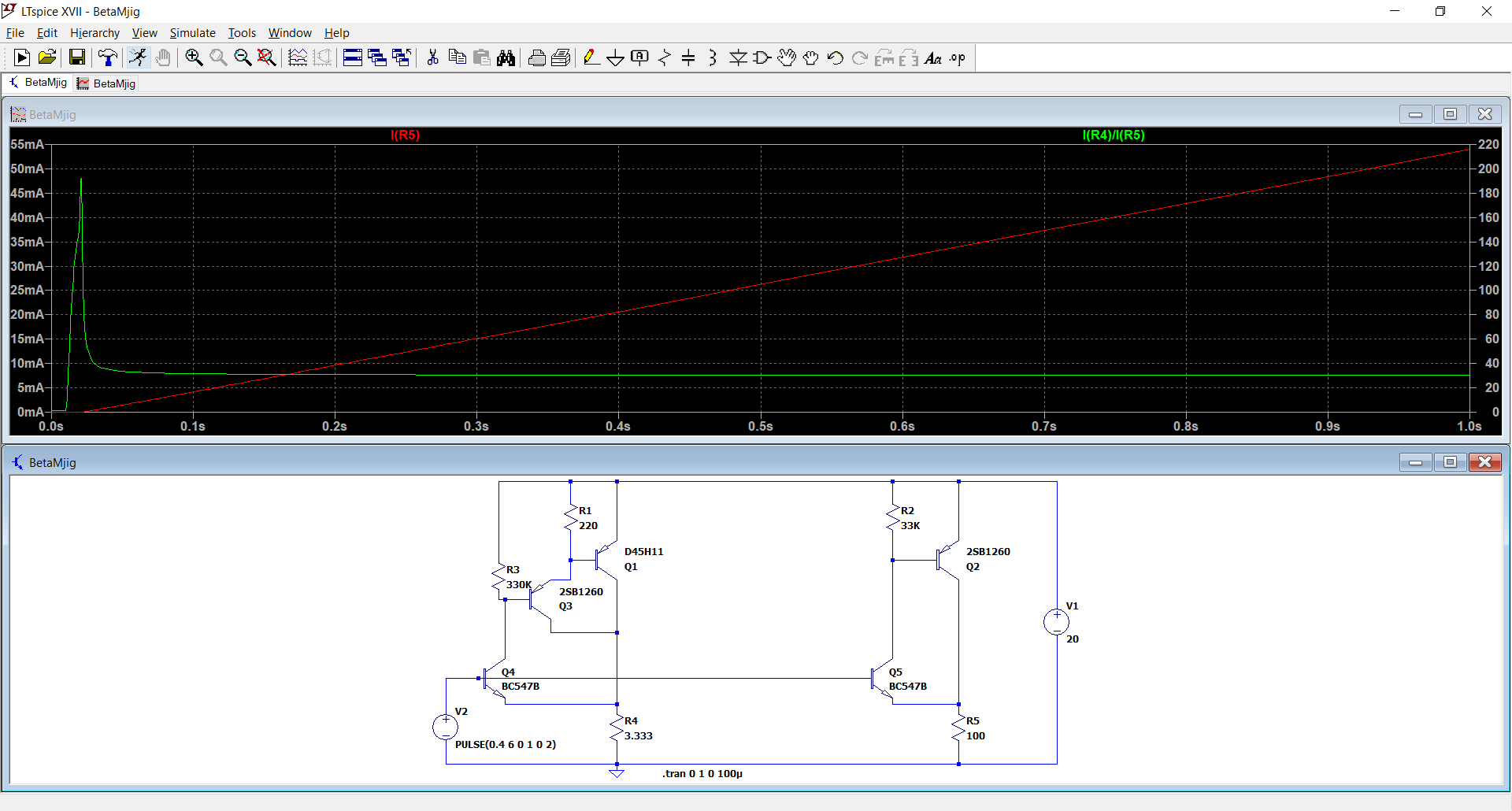
Note that the problem is not the huge spike at the start (it happens when both sides are cutoff), but the region that immediately follows, where the deviation from the ideal ratio is several percents.
The problem is caused by the Vbe delta between Q4 and Q5, which originates from different emitter currents.
The difficulty is to match emitter currents for all working conditions
Attachments
I suspect some form of op-amp might be necessary with such a large magnification ratio.
(You don't happen to know any nearby semiconductor companies do you? They could easily place 101 devices in an array in a chip!)
It would be possible to use a diff amp with PNP darlingtons on the input to feed an NPN, then PNP current multipliers. The whole thing could run from a single rail.
(You don't happen to know any nearby semiconductor companies do you? They could easily place 101 devices in an array in a chip!)
It would be possible to use a diff amp with PNP darlingtons on the input to feed an NPN, then PNP current multipliers. The whole thing could run from a single rail.
I suspect some form of op-amp might be necessary with such a large magnification ratio.
(You don't happen to know any nearby semiconductor companies do you? They could easily place 101 devices in an array in a chip!)
It would be possible to use a diff amp with PNP darlingtons on the input to feed an NPN, then PNP current multipliers. The whole thing could run from a single rail.
Do you perhaps know names of any good semiconductor companies that you could share?
Interesting.
I need to see how to incorporate it in in the circuit, and how it will behave with a phantom polarity overlaid, but it is certainly worth examining
It will be my fallback solution if nothing better emerges
I need to see how to incorporate it in in the circuit, and how it will behave with a phantom polarity overlaid, but it is certainly worth examining
Yes, I considered it and provisionally rejected it because of the (relative) complexity. It would also have to cope with both polarities.It would be possible to use a diff amp with PNP darlingtons on the input to feed an NPN, then PNP current multipliers. The whole thing could run from a single rail.
It will be my fallback solution if nothing better emerges
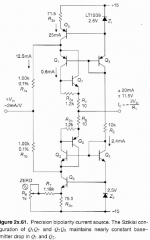
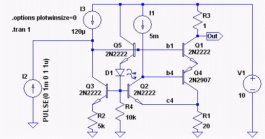
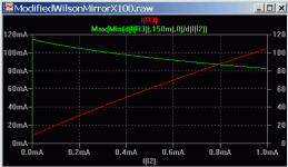
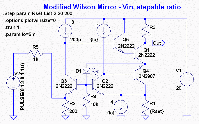
Modified Wilson mirror for x100
Hi Elvee,
Attached circuits for x10 and x100.

.
I2 provides bias for Q2 for better linearity. Not perfectly linear") . (Quite OK for some applications. I used it to sense differnetial voltage (across a 50mR sense resistor) at the ground points of R2 and R1).
. (Quite OK for some applications. I used it to sense differnetial voltage (across a 50mR sense resistor) at the ground points of R2 and R1).
I3 zeros out offsets bias voltage on R1.
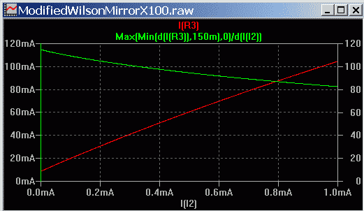
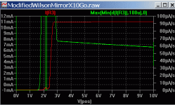
With up to 1V developed on R1 you need about 3V headroom. See 3rd plot (also plots output conductance).
Hi Elvee,
Attached circuits for x10 and x100.
.
I2 provides bias for Q2 for better linearity. Not perfectly linear
. (Quite OK for some applications. I used it to sense differnetial voltage (across a 50mR sense resistor) at the ground points of R2 and R1).I3 zeros out offsets bias voltage on R1.
With up to 1V developed on R1 you need about 3V headroom. See 3rd plot (also plots output conductance).
Attachments
Thanks for your efforts, unfortunately the topology isn't well suited to multiple ranges/wide dynamic range.Hi Elvee,
Attached circuits for x10 and x100.
.
I2 provides bias for Q2 for better linearity. Not perfectly linear
I3 zeros out offsets bias voltage on R1.
With up to 1V developed on R1 you need about 3V headroom. See 3rd plot (also plots output conductance).
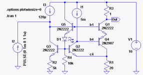
This is the high-current setting (the sim has some problems):
The low current sim doesn't work, but it is obvious that switching I1 --> I4 and R2, R6 for each range would be required:
Attachments
Hi Elvee,
Does this help?
.
Now voltage input and stepable ratio using R1.
I4 removes offset voltage on R1 so I1 and I3 don't need stepping.
Q5 is now a Darlington. I3 is set so there is enough drive for the Darlington to give the highest output current through R3. D1 is now driven from emitter of Q1. R4 can be removed now (I think?).
Attachments

I need to evaluate the circuit in details, but the presence of Io will be problematic.
The Ic generator spans 50µA to 5A in 4 ranges, and the Ib generator 0.5µA to 50mA.
The accuracy of Io would need to be exceptional.
In addition, there is no negative supply, and creating a Io capable of operating down to zero volt, like a spice source looks insurmountable.
Note that absolute accuracy or linearity is unimportant: only a perfect 1:100 tracking matters
Hi Elvee,
------
Like John Ellis Post 6 an opamp would simplify the problem for wide ranges. A DCDC converter can give the +/- rails for the opamp.
Sqitching in your circuit may be limiting your circuit options -- so what about a hardwired version for NPN and another for PNP without any NPN/PNP switching? Either both in the same enclosure or separate enclosures.
An isolated 1W DC-DC converter could be used for I1 and then I4 would not be needed since a floating CCS negative can be connected to Q2 emitter. If you use an unregulated converter they are inexpensive, then add an IC regulator and a resistor and you have a CCS (or use the IC Vreg as a CCS).... there is no negative supply, and creating a Io capable of operating down to zero volt, like a spice source looks insurmountable.
------
Like John Ellis Post 6 an opamp would simplify the problem for wide ranges. A DCDC converter can give the +/- rails for the opamp.
Sqitching in your circuit may be limiting your circuit options -- so what about a hardwired version for NPN and another for PNP without any NPN/PNP switching? Either both in the same enclosure or separate enclosures.
As I couldn't find a better alternative, I resigned myself to using an opamp.
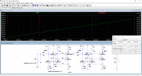
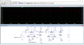
Unfortunately, it isn't the end of the story yet: the basic diff-amp doesn't have enough gain for a sufficient accuracy. The ratio deviates from 100 at high and low currents:
This means further complications (and transistor matching):
I now have to check that the circuit can still work satisfactorily with the ghost, opposite polarity in parallel.
In the meantime, if someone has a bright idea to overcome the gain problem more simply and effectively, I would gladly welcome it
Attachments
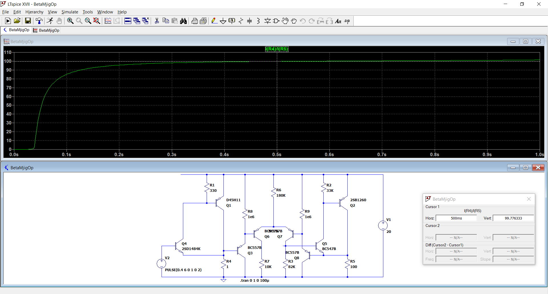
A circuit very similar to the one I had thought of, but for a few points:
I ran the tail current of the differential amp at 2mA. This was fed through a CCS.
Your R3, R7 would have to be reduced.
Input side directly to 100 ohms (no Q4, Q1, R4=100). Feedback side (your Q8) fed through 99 ohm resistor to a 1 ohm load (giving 100x gain). The 99 ohms is to balance the input-feedback side impedances. Seems to me that you had the reverse gain in mind from your circuit?
Your Q5 operated with emitter grounded and a Darlington for Q2.
Also a small trimpot in the differential emitter stage to balance.
Main point is that for good gain linearity both sides of the diff amp need to be balanced exactly. That means, as you say, the transistors have to be matched in the corresponding pairs (Q6-Q7; Q3-Q8; Q9-Q10) in both Vbe and hfe, and for linearity both sides need to have identical impedances (connecting the emitter of Q5 to Q8 may upset this, as do the unbalanced impedances (1 ohm one side 100 the other).
Not sure if that helps, but when needing precision, op amps need precision matching and balancing.
That's pretty much what I thought of except I also had a current mirror instead of R3/R7, as you did in one of your earlier posts. Otherwise there might be an imbalance in the currents in Q6/Q7.
The Vbe of Q4 will generate a non-linear component to the input, but I guess you will work with that.
The Vbe of Q4 will generate a non-linear component to the input, but I guess you will work with that.
- Status
- This old topic is closed. If you want to reopen this topic, contact a moderator using the "Report Post" button.
- Home
- Amplifiers
- Solid State
- Ideas for better CCS tracking?