As I have been saying on many threads, I am only interested in Class B amplifiers.
However, people in this forum as well as everywhere consider Class B amplifiers a crime against audio, because of their crossover delay and non linearity.
Although these can be tackled to an extend, people prefer to use extra circuitry to convert Class B amplifiers into Class AB.
Thus, I have decided to make a circuit without resistors on the path of the base currents of the output transistors, something, which I have decided to call " Enigma Machine ".
I think, I have been able to make and test the said circuit, a schematics of which is at the addendum of this document, just after the explanation of the said circuit.
Here is the document :
A Buffer for Class AB Amplifiers - Google Drive
Technically class B has 180 degree conduction angle per device - commoning bases and emitters like that circuit is actually class C (or perhaps BC), less than 180 degree conduction, and never satisfactory apart from quiescent power consumption being low. Heavy distortion happens at small signal levels, spraying harmonics all up the spectrum to ultrasonic frequencies and beyond.
Biasing a circuit to class B involves setting the queiscent current to a fairly precise value to minimize crossover distortion, about 50mA for EF output stages, 100mA for MOSFET source followers, and perhaps about 10mA for a CFP output stage. The hard part of class B design is stabilizing the optimum bias as parts heat up and cool down - often not presented in the amp's specs, alas, as its crucial.
Class AB bias is where the current is substatially higher than this, and doesn't minimize crossover distortion, it instead prevents crossover distortions appearing below a certain power threshold.
So for AB, the devices are in class A for small signals, but have crossover at higher levels, and usually quite a bit more crossover distortion then than a class B bias would have.
I gave up trying to figure out which part of that long document you are refering too - can you post it directly?
Technically class B has 180 degree conduction angle per device - commoning bases and emitters like that circuit is actually class C (or perhaps BC), less than 180 degree conduction, and never satisfactory apart from quiescent power consumption being low. Heavy distortion happens at small signal levels, spraying harmonics all up the spectrum to ultrasonic frequencies and beyond.
Biasing a circuit to class B involves setting the queiscent current to a fairly precise value to minimize crossover distortion, about 50mA for EF output stages, 100mA for MOSFET source followers, and perhaps about 10mA for a CFP output stage. The hard part of class B design is stabilizing the optimum bias as parts heat up and cool down - often not presented in the amp's specs, alas, as its crucial.
Class AB bias is where the current is substatially higher than this, and doesn't minimize crossover distortion, it instead prevents crossover distortions appearing below a certain power threshold.
So for AB, the devices are in class A for small signals, but have crossover at higher levels, and usually quite a bit more crossover distortion then than a class B bias would have.
I gave up trying to figure out which part of that long document you are refering too - can you post it directly?
1. Power amplifier classes - Wikipedia
2. The circuit can be tuned to provide any output voltage difference and, thus, collector emitter currents at 0V.
3. The document is long, true, however, the relevant chapter is the last chapter called " Enigma Machine ". This chapter is also long, thus, the schematics are in the addendum. There are a few schematics, true, thus, for a quick browse, look at the last schematics on the last page of the document.
The document has been updated with a new point, called " Real Range ", which is inserted just before the Schematics.
I think, I have found some tiny mistakes in the document too, I would try to correct. Can be read as is, except the document is long and the length will not be decreased.
I think, I have found some tiny mistakes in the document too, I would try to correct. Can be read as is, except the document is long and the length will not be decreased.
Semantics
Wikipedia Amplifier Classes (link above) defines Class-AB as optimal biased with a small current.
Mark's post 2 above calls this "Class-B" as per Douglas Self, which is at odds with the long standing one. See Post 135 here and Post 140 here.
Wikipedia Amplifier Classes (link above) defines Class-AB as optimal biased with a small current.
Mark's post 2 above calls this "Class-B" as per Douglas Self, which is at odds with the long standing one. See Post 135 here and Post 140 here.
Everyone has generally considered the "optimal class-B" biasing to be class-AB until Doug presented his definition. Truly, that is what confuses many about the A,B,AB debate.
Steven,
Have you seen Faran and Falks Class-B amp? It is similar to your Fig 7.4 p57. Faran J. J. Jr, Fulks R. G, 'High-Impedance Drive for the Elimination of Crossover Distortion', IRE Trans. Audio, Jul/Aug 1962 p99-105. IRE_Faran_High-Impedance-Drive-Elimination-Crossover-Distortion_Jul-1962.pdf - Google Drive

If you use LTspice a sim file is here.
Also have you seen Malcolm Hawksfords Class-B output stage?

His article can be viewed here. Some food-for-thought maybe.
There is also the Blomley Class-B. LTspice can generate audio files of simulations so you can listen to music through your virtual circuits. Files for Blomley virtual listener testing were posted here.
There is the recent Class-B design by LKA here
Your machine-gun noise (p104) is interesting. Maybe a simulation can uncover its cause and find a cure.
I have a hunch that its an electrothermal instability and will require electrothermal models for the power transistors and maybe diodes. Ordinary models are isothermal - their temperature stays absolutely constant during each run. SPICE was designed like that because electrothermal models were difficult to model and run slow (and they still are).
Have you seen Faran and Falks Class-B amp? It is similar to your Fig 7.4 p57. Faran J. J. Jr, Fulks R. G, 'High-Impedance Drive for the Elimination of Crossover Distortion', IRE Trans. Audio, Jul/Aug 1962 p99-105. IRE_Faran_High-Impedance-Drive-Elimination-Crossover-Distortion_Jul-1962.pdf - Google Drive
If you use LTspice a sim file is here.
Also have you seen Malcolm Hawksfords Class-B output stage?
His article can be viewed here. Some food-for-thought maybe.
There is also the Blomley Class-B. LTspice can generate audio files of simulations so you can listen to music through your virtual circuits. Files for Blomley virtual listener testing were posted here.
There is the recent Class-B design by LKA here
Your machine-gun noise (p104) is interesting. Maybe a simulation can uncover its cause and find a cure.
I have a hunch that its an electrothermal instability and will require electrothermal models for the power transistors and maybe diodes. Ordinary models are isothermal - their temperature stays absolutely constant during each run. SPICE was designed like that because electrothermal models were difficult to model and run slow (and they still are).
Attachments
Last edited:
Hi Holmer,
As far as I can interpret Steven's aim, he is "only interested in Class-B" (see post1).
Not the standard "optimum bias" with diodes or Vbe multiplier or spreader that gives what is usually called "Class-AB".
The title used for this thread seems to be misleading .
.
Maybe it should be changed to: "A Buffer for Class-B Amplifiers"
As far as I can interpret Steven's aim, he is "only interested in Class-B" (see post1).
Not the standard "optimum bias" with diodes or Vbe multiplier or spreader that gives what is usually called "Class-AB".
The title used for this thread seems to be misleading
. Maybe it should be changed to: "A Buffer for Class-B Amplifiers"
And this is why I do not like terms.
I do NOT use terms, but, some people do. This is why I decided to use them now and I realised this mistake. When I use terms, I use only Wikipedia terms, because, they are the only standard ones. Of course, everyone can make their own terms.
As per Wikipedia, Class B amplifiers are only the push pull buffer amplifier WITHOUT any offset bias. The better way to say is : " Amplifiers with Push Pull Buffer Output Stages without Any Offset Bias ". These are the ONLY amplifiers I am interested in. I have made one and published the document under the thread called " Amplifier ", in this forum.
As per Wikipedia, Class AB amplifiers are all amplifiers with an offset bias to the output push pull stage. Regardless of whether they provide some offset bias, insufficient to keep the transistors fully open or whether the transistors are kept very well open. The schematics are the same, regardless of whether only the current through the offset bias circuit is increased or diodes are replaced or new diodes are inserted or transistors in diode configurations with collector and base connected are inserted. Still, they are the same. These should be called " Amplifiers with Push Pull Buffer Output Stages with Some Offset Bias ".
Although I am only interested in " Voltage Amplifiers with Push Pull Buffer Output Stages without Any Offset Bias ", I have decided to make a schematics which I have inserted between the IC amplifier and the output stage, in order to make an " Voltage Amplifier with Push Pull Buffer Output Stages with Some Offset Bias ".
Again, I am only interested in fully voltage amplifiers and not in current amplifiers, nor amplifiers with voltage to current converters.
The whole amplifier is on modular principle : I can add this circuit, which is on a separated PCB or I can remove this circuit whenever I want. Just a question of reconfiguring wires on a connector which has screws to support the wires.
So, the amplifier without any offset bias circuit was made before. Now, the circuit which provides offset bias to this amplifier was made separately and inserted just before the output stage.
One of the reasons to make this circuit was for this forum. People here do not seem to like push pull output stages without any offset bias because of the crossover.
The document starts with an introduction to the previous schematics without the offset bias circuit. Then, the document discusses standard approaches. The, only the last chapter, called " Enigma Machine " is dedicated to the circuit which provides offset bias.
The offset bias is adjustable and can provide voltages which do not open the transistors, but, keep them at the border between open and closed at crossover. Also, the offset bias can be adjusted to keep the transistors open. Also, diodes can be replaced, other diodes and or transistors in diode configurations with collector and base connected can be added. Thus, any voltage can be made.
The voltage is temperature and current dependent. Some compensation has been provided and discussed. The most important point is to adjust the voltage at crossover, around 0V.
The document is very long. Thus, there are some options :
1. Read the whole document. Unlikely.
2. Read only the chapter " Enigma Machine ". Also very long.
3. Look at the schematics at the addendum :
3a. Look at all schematics. These provide ideas and tests. Also very long.
3b. Look at all schematics, except the first one. Also very many.
3c. Look only at the very last schematics.
Most of you would chose 3c.
Again, the circuit has been made and tested. The tests were two types :
1. A DC test. DC voltages were applied and the circuit was measured with a multimeter.
2. Real tests, but, only with the said platform made before. No signal generators, no oscilloscopes, nothing. Just play sound. The only measurement equipment available was a digital multimeter. Nothing else.
Summary :
1. What to look at : Look at the last page only. Those who want can read more as mentioned.
2. What am I interested in : Pure voltage amplifiers with and IC amplifier and an NPN PNP buffer without any offset bias. Of course, any voltage amplifier is nice.
Last edited:
The document has been updated. I have corrected some mistaken schematics where the positive and negative input of the IC amplifier were mistaken because of copy and paste.
I have done some other corrections.
I have added some more stuff, such as Figure 2.3 and explanations thereof.
I have done some other corrections.
I have added some more stuff, such as Figure 2.3 and explanations thereof.
Here is the OLD post, which discusses the amplifier without any offset bias. :
Amplifier
This amplifier was used as the platform where the new circuit was inserted. By adjusting the current with the trimmer, offset voltages can be provided which cover some range, good enough to provide tiny amounts of offset bias voltages as well as bigger ones. Simple Replacements and or insertion of diodes, transistors in diode configuration with connected base and collector can be used to make any offset bias voltages.
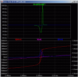
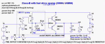
Effect of an pamps first pole on unbiased Class-B jump distortion
Hi Steve,
Continuing simulations with no bias and a fast opamp. This post is with an output pole in my opamp model closer to the LM7171 first pole.
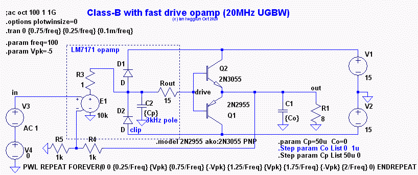
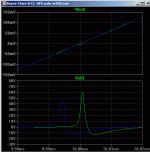
The pole capacitor was set for 3kHz using an AC run with R4 removed (open-loop). With Avol of 80dB the unity gain frequency for this model is found to be 20MHz. The value of Cp can be stepped so the effect of this pole can be seen on plots (below) for a 5V input 100Hz triangle wave of 100Hz:
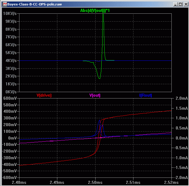
The top pane is the gm variation in the crossover region: Blue is without the pole and Green is with 20MHz GBW.
Lower pane shows the base drive voltage moving through the "jump" region and the drive current. BTW The transistor capacitance in this region is the drive current divided by the slope of the drive voltage, it appears to be around 2nF. The opamp pole lengthens the transition and reduces the slope (less drive current flows).
Now the effect of the opamp pole on distortion readings with 5Vpk input, 100Hz, sine (below)

The upper pane shows the output voltage in the crossover region, Green with the pole.
The lower pane shows the output voltage of the weighting filer which boosts the higher harmonics like our ear. Green is with the pole, delayed and slightly larger but not by much.
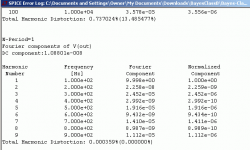
The weighted THD and unweighted readings with the pole are below:

.
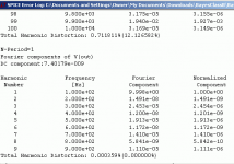
And with no pole the values are almost identical:

.
The weighted distortion, if it can be believed, suggests the huge gain variations when the pole is added (seen in the first triangle wave plots) hardly affects what we would hear as crossover distortion when no bias is used with a fast opamp. Listener tests are need to verify this, preferably using bench tests.
The simulated distortion test circuit is also included in the attached zip for a short clean guitar strum for those interested if the crossover distortion is audible with music and what type of music makes it most noticeable.
Lastly, adding output capacitance causes oscillation when the series resistance (ESR) is less than 0.3 ohms and Co is more than 200nF with this model. With a 1uF output capacitor the series resistance needs to be more than 0.5 ohms to stop oscillation with this model. The frequency of oscillation was around 500kHz.
Hi Steve,
Continuing simulations with no bias and a fast opamp. This post is with an output pole in my opamp model closer to the LM7171 first pole.
The pole capacitor was set for 3kHz using an AC run with R4 removed (open-loop). With Avol of 80dB the unity gain frequency for this model is found to be 20MHz. The value of Cp can be stepped so the effect of this pole can be seen on plots (below) for a 5V input 100Hz triangle wave of 100Hz:
The top pane is the gm variation in the crossover region: Blue is without the pole and Green is with 20MHz GBW.
Lower pane shows the base drive voltage moving through the "jump" region and the drive current. BTW The transistor capacitance in this region is the drive current divided by the slope of the drive voltage, it appears to be around 2nF. The opamp pole lengthens the transition and reduces the slope (less drive current flows).
Now the effect of the opamp pole on distortion readings with 5Vpk input, 100Hz, sine (below)
The upper pane shows the output voltage in the crossover region, Green with the pole.
The lower pane shows the output voltage of the weighting filer which boosts the higher harmonics like our ear. Green is with the pole, delayed and slightly larger but not by much.
The weighted THD and unweighted readings with the pole are below:
.
And with no pole the values are almost identical:
.
The weighted distortion, if it can be believed, suggests the huge gain variations when the pole is added (seen in the first triangle wave plots) hardly affects what we would hear as crossover distortion when no bias is used with a fast opamp. Listener tests are need to verify this, preferably using bench tests.
The simulated distortion test circuit is also included in the attached zip for a short clean guitar strum for those interested if the crossover distortion is audible with music and what type of music makes it most noticeable.
Lastly, adding output capacitance causes oscillation when the series resistance (ESR) is less than 0.3 ohms and Co is more than 200nF with this model. With a 1uF output capacitor the series resistance needs to be more than 0.5 ohms to stop oscillation with this model. The frequency of oscillation was around 500kHz.
Attachments
-
 Bayes-Class-B-CC-OPS-pole5V-100HzTri.png8.5 KB · Views: 1,270
 -
 Bayes-Class-B-CC-OPS-nopole5V-100Hz-wTHDlog.png6.6 KB · Views: 1,241
 -
 Bayes-Class-B-CC-OPS-pole5V-100Hz-wTHDlog.png6.9 KB · Views: 1,255
 -
 Bayes-Class-B-CC-OPS-pole5V-100Hz-wTHD.png6.6 KB · Views: 1,263
 -
 Bayes-Class-B-CC-OPS-pole.png24.6 KB · Views: 1,358
 -
Bayes-Class-B-CC-OPS-pole.zip88.7 KB · Views: 66
This is an amazing post, but,
1. The place to post this post is in the other thread called " Amplifier ", because this thread concerns the schematics which provides offset bias to the power transistors.
2. The analysis is rather complicated, yet, very thorough and I do thank you very much for this. However, the most important question I have to you is this :
Apply a square wave voltage at the very input of LM7171. The choice of amplitude and frequency is yours. How long after the input square wave voltage changes from one amplitude to another does the overall system take to make the output reach the corresponding voltage?
2a. The measurements are to be made without the output capacitor Co
2b. The measurements are to be made with Co = 1uF
I will be extremely grateful in case you can post two graphics, one for 2a and one for 2b, each of which contains only input and output voltage, Ui and Uo.
Please, do not put any filters or other components between LM7171 and the transistors.
Anyway, you have provided a piece of outstanding work. Thank you again.
Although I cannot understand most of the work, looks like, without the 2N2222A 2N2907 buffer, I have not been able to achieve what I wanted to achieve. And what I wanted to achieve is a transient period of 250ns or lower at some amplitude near the worst case, i. e., low amplitude.
Another point I am unable to understand is why you say Cp is adjustable and the schematics says Cp is internal to LM7171?
Please inform.
Also, you have mentioned the input capacitance of the power transistors is around 2nF. I expected around 1nF. However, there are similar Toshiba transistors which give 600pF.
Another point is LM7171 can supply more than 100mA of current. I am not sure whether the emulation software is aware of this and other parameters of LM7171.
Anyway. Thanks. Can your post and this reply be moved to the other thread?
A document, called Errata.doc has been published here : Errata - Google Drive
The document correct errors I may have made in various projects I have worked on.
The document is to be updated.
Please, report all errors and problems.
The document correct errors I may have made in various projects I have worked on.
The document is to be updated.
Please, report all errors and problems.
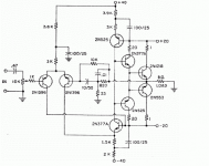
Buffer for Class AB Amplifiers with Adders
I have designed another buffer for Class AB amplifiers based on adders. I always prefer to first make and test the schematics before I post here, however, I consider this design very important and, therefore, want to first publish the idea in this case.
This design is fully symmetrical : whatever happens with the NPN transistor, happens with the PNP transistor. The only asymmetry comes from the general differences between an NPN transistor and the complementary, PNP, transistor.
Most importantly, there are no resistors before the power transistors, only before the low capacitance buffer transistor. The resistor values depends on the amplifier's output.
The idea can be accomplished fully by amplifiers, yet, the schematics show the transistor approach.
Some explanations :
I discussed the difficulty to make an equal control of the push pull output buffer transistors. The standard schematics uses a current source and a transistor ( in something like a common collector configuration, without a base resistor ). The current source and the transistor control the push pull output, yet, not evenly : at one of the extremes, the transistor will be nearly or fully closed and the current source will control one of the push pull transistors. In the other extreme, the transistor will be fully open and this fully open transistor will control the other push pull transistor. Thus, one of the transistors can get a good base current and the other, only the current provided by the current source.
I then made a schematic with three transistors to mitigate the problem to some extent.
Yet, now, I think, I have solved the problem.
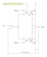
I decided to use two adders and add offset directly to them. The price to pay is slightly reduced maximum voltage and, worse, the transistor which buffers the adder needs to have a high input impedance. Not so bad, though. The picture called " Amplifier Transistor Adder with Sziklais. jpg " shows this.
Now, as you have pointed out, when the temperature changes, the Ube of the adder transistor changes. The use of Sziklais mitigates this problem to some extent ( and requires only 0.7V offset ). Temperature compensation is needed.
The best temperature compensation is to model the behaviour of the compensated transistor with thermistors. True, the temperature of the compensated transistor varies with the load, yet, some average modeling may be possible.
Also, when the transistor gets very hot, either the ambient temperature is high or the transistor dissipates a lot of power. In case of the second, this means the signal is high. When the signal is high, the slope of the signal when the signal goes over 0V is steep. The steep slope requires higher current at 0V for a better linearity. Thus, the increased temperature, caused by the transistor's dissipation will make the Ube of the transistor lower at the same offset and, therefore, the current through the transistor will be higher. The thermal runaway ( positive temperature feedback ) seems to, even, help this way! : )
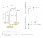
Anyway, the picture, called, " Simple Temperature Compensation 2.jpg " shows a possible, yet, niot perfect compensation.
A diode voltage is amplified. This is the offset. However, the adder attenuates the offset. When the amplification is equal to 1 / the attenuation, the voltage at the base of the transistor will be nearly Ua + 0.7V. In case Ube of the transistor changes because of the ambient ( or other ) temperature, then, the diode voltage of around 0.7V will also change because of the temperature. Well, not exactly the same, but, somewhat.
In the pictures, the condition is Rc1 / Re1 = 1 + R11 / R12.
Simple example. The diode voltage is 0.7V. Make Rc1 / Re1 = 20. Then, Uoffpos = 0.7 * 20 = 14V. Then, make R11 / R12 = 19. Then, the base of T10 will have Ua / ( 1 + 1 / 19 ) + 0.7 = 0.95 * Ua + 0.7!
The attenuation 0.95 will be covered by the amplifier, but, reduces the maximum voltage. In case the amplifier is powered by, say, +- 16.5V and can only reach 1.5V off the rails, which, is 15V, the attenuation will reduce these 15V to 0.95 * 15 = 14.25V, i. e., by 0.75V. Not so bad, though. The transistor will make another reduction of 0.7V. When there are Darlingtones, the numbers are higher. This is another advantage of the Sziklais. One can put many transistors in Darlington configuration for the Sziklai transistor. The control transistor remains one only and consumes one Ube of the maximum voltage only.
Of course, the sensitivity problem may be slightly exacerbated in cases of high Beta. And, a somewhat higher Beta is necessary not to shunt the adder resistors, which, are limited by the amplifier. With temperature, not only Ube decreases, but, Beta increases. Thus, with a very high overall Beta, tiny changes of temperature may bring high changes in the current.
Interesting : the offset transistor can only source current and not sink. This, however, seems to be an advantage. The offset will only source current, because the offset has to be as high as possible, close to Vcc ( minus Ucesat of the control transistor ). However, when Ua becomes higher than the offset ( minus 0.7 ), then, there will not be an offset. Yes, but, offset is needed only at 0V ( bonus : around 0V the current is low and Beta is high as opposed to at very high currents ( voltages ) ). The lack of offset at high voltages means there will be one limitation fewer for the maximum voltage ( although some of the limitations overlap ). And there will be plenty of a period ( 12.5us at 20KHz ) for the offset to set again before the next 0V is reached. Or the sink problems must be corrected.
The picture " Simple Temperature Compensation 2.jpg " also shows how the offset can be achieved with an amplifier. Much better and easier. Can be with or without sinking ( there will not be sinking with an output transistor ). Cannot put very many filters, though. Also, since an amplifier has been used, the adder, best, be made with an amplifier too, which, is, also, the better possibility. This has been addressed in the article which I have not fully written on the subject.
Again :
I am worried of the requirement for low current at the base of the first transistor. Without the adder, one does not need such high Beta, because, the amplifier supplies the base current ( although the maximum voltage of the output of the amplifier decreases with the increase of the output current ). However, with the adder, the amplifier runs the resistors of the adder. Their overall value must not be very low. Then, the buffer must not consume significant current. This current depends not only on the load and the overall Beta, but, also, on the quiescent current, the current through the push pull transistors at 0 output voltage.
Usually, in some cases, this means another transistor, the adder's buffer transistor, is necessary. Also, this means a higher sensitivity : a tiny increase of temperature may bring high increase in output current. Similarly, a decrease of temperature to the commercial 0°C means an increase of current. Assuming Ube = 0.65V at 25°C, Ube changes between 0.7V at 0°C and 0.55V. So, the offset may be insufficient at 0°C or huge at 0.55°C.
In other words, the standard schematics uses a transistor to control low Beta output transistors and the changes of Ube are not a big deal. This schematics, however, controls a higher Beta transistors and Ube variations can be significant.
The only advantage is the said temperature dependence introduces higher quiescent current at high output, where the slope of the output voltage is high and smoother go through 0V is required.
A trimmer ( s ) is a must. A good idea is to use the input impedance of the buffer transistor of the adder. I have the formula, but, did not want to use for the preliminary discussion.
I have designed another buffer for Class AB amplifiers based on adders. I always prefer to first make and test the schematics before I post here, however, I consider this design very important and, therefore, want to first publish the idea in this case.
This design is fully symmetrical : whatever happens with the NPN transistor, happens with the PNP transistor. The only asymmetry comes from the general differences between an NPN transistor and the complementary, PNP, transistor.
Most importantly, there are no resistors before the power transistors, only before the low capacitance buffer transistor. The resistor values depends on the amplifier's output.
The idea can be accomplished fully by amplifiers, yet, the schematics show the transistor approach.
Some explanations :
I discussed the difficulty to make an equal control of the push pull output buffer transistors. The standard schematics uses a current source and a transistor ( in something like a common collector configuration, without a base resistor ). The current source and the transistor control the push pull output, yet, not evenly : at one of the extremes, the transistor will be nearly or fully closed and the current source will control one of the push pull transistors. In the other extreme, the transistor will be fully open and this fully open transistor will control the other push pull transistor. Thus, one of the transistors can get a good base current and the other, only the current provided by the current source.
I then made a schematic with three transistors to mitigate the problem to some extent.
Yet, now, I think, I have solved the problem.
I decided to use two adders and add offset directly to them. The price to pay is slightly reduced maximum voltage and, worse, the transistor which buffers the adder needs to have a high input impedance. Not so bad, though. The picture called " Amplifier Transistor Adder with Sziklais. jpg " shows this.
Now, as you have pointed out, when the temperature changes, the Ube of the adder transistor changes. The use of Sziklais mitigates this problem to some extent ( and requires only 0.7V offset ). Temperature compensation is needed.
The best temperature compensation is to model the behaviour of the compensated transistor with thermistors. True, the temperature of the compensated transistor varies with the load, yet, some average modeling may be possible.
Also, when the transistor gets very hot, either the ambient temperature is high or the transistor dissipates a lot of power. In case of the second, this means the signal is high. When the signal is high, the slope of the signal when the signal goes over 0V is steep. The steep slope requires higher current at 0V for a better linearity. Thus, the increased temperature, caused by the transistor's dissipation will make the Ube of the transistor lower at the same offset and, therefore, the current through the transistor will be higher. The thermal runaway ( positive temperature feedback ) seems to, even, help this way! : )
Anyway, the picture, called, " Simple Temperature Compensation 2.jpg " shows a possible, yet, niot perfect compensation.
A diode voltage is amplified. This is the offset. However, the adder attenuates the offset. When the amplification is equal to 1 / the attenuation, the voltage at the base of the transistor will be nearly Ua + 0.7V. In case Ube of the transistor changes because of the ambient ( or other ) temperature, then, the diode voltage of around 0.7V will also change because of the temperature. Well, not exactly the same, but, somewhat.
In the pictures, the condition is Rc1 / Re1 = 1 + R11 / R12.
Simple example. The diode voltage is 0.7V. Make Rc1 / Re1 = 20. Then, Uoffpos = 0.7 * 20 = 14V. Then, make R11 / R12 = 19. Then, the base of T10 will have Ua / ( 1 + 1 / 19 ) + 0.7 = 0.95 * Ua + 0.7!
The attenuation 0.95 will be covered by the amplifier, but, reduces the maximum voltage. In case the amplifier is powered by, say, +- 16.5V and can only reach 1.5V off the rails, which, is 15V, the attenuation will reduce these 15V to 0.95 * 15 = 14.25V, i. e., by 0.75V. Not so bad, though. The transistor will make another reduction of 0.7V. When there are Darlingtones, the numbers are higher. This is another advantage of the Sziklais. One can put many transistors in Darlington configuration for the Sziklai transistor. The control transistor remains one only and consumes one Ube of the maximum voltage only.
Of course, the sensitivity problem may be slightly exacerbated in cases of high Beta. And, a somewhat higher Beta is necessary not to shunt the adder resistors, which, are limited by the amplifier. With temperature, not only Ube decreases, but, Beta increases. Thus, with a very high overall Beta, tiny changes of temperature may bring high changes in the current.
Interesting : the offset transistor can only source current and not sink. This, however, seems to be an advantage. The offset will only source current, because the offset has to be as high as possible, close to Vcc ( minus Ucesat of the control transistor ). However, when Ua becomes higher than the offset ( minus 0.7 ), then, there will not be an offset. Yes, but, offset is needed only at 0V ( bonus : around 0V the current is low and Beta is high as opposed to at very high currents ( voltages ) ). The lack of offset at high voltages means there will be one limitation fewer for the maximum voltage ( although some of the limitations overlap ). And there will be plenty of a period ( 12.5us at 20KHz ) for the offset to set again before the next 0V is reached. Or the sink problems must be corrected.
The picture " Simple Temperature Compensation 2.jpg " also shows how the offset can be achieved with an amplifier. Much better and easier. Can be with or without sinking ( there will not be sinking with an output transistor ). Cannot put very many filters, though. Also, since an amplifier has been used, the adder, best, be made with an amplifier too, which, is, also, the better possibility. This has been addressed in the article which I have not fully written on the subject.
Again :
I am worried of the requirement for low current at the base of the first transistor. Without the adder, one does not need such high Beta, because, the amplifier supplies the base current ( although the maximum voltage of the output of the amplifier decreases with the increase of the output current ). However, with the adder, the amplifier runs the resistors of the adder. Their overall value must not be very low. Then, the buffer must not consume significant current. This current depends not only on the load and the overall Beta, but, also, on the quiescent current, the current through the push pull transistors at 0 output voltage.
Usually, in some cases, this means another transistor, the adder's buffer transistor, is necessary. Also, this means a higher sensitivity : a tiny increase of temperature may bring high increase in output current. Similarly, a decrease of temperature to the commercial 0°C means an increase of current. Assuming Ube = 0.65V at 25°C, Ube changes between 0.7V at 0°C and 0.55V. So, the offset may be insufficient at 0°C or huge at 0.55°C.
In other words, the standard schematics uses a transistor to control low Beta output transistors and the changes of Ube are not a big deal. This schematics, however, controls a higher Beta transistors and Ube variations can be significant.
The only advantage is the said temperature dependence introduces higher quiescent current at high output, where the slope of the output voltage is high and smoother go through 0V is required.
A trimmer ( s ) is a must. A good idea is to use the input impedance of the buffer transistor of the adder. I have the formula, but, did not want to use for the preliminary discussion.
Attachments
Again, there are two, extremely, important considerations :
1. When Re3 is very high or infinity ( not installed ), and the amplifier can reach higher voltages than Ue3, then, there is no loss of maximum voltage, because, the transistor T3 cannot sink current and is closed. The price to pay is a slow, non linear control at the point when T3 becomes closed, which, the amplifier will cover for.
2. The β of the output transistors decreases with their collector emitter currents, yet, the only place of interest is around 0V, where, the collector emitter currents are low and the β of the output transistors and thus, the overall β is high.
Therefore, there is no disadvantage of this approach, except, the necessity of a higher, overall β, which, however, reduces the consumption of current from the amplifier and allows the amplifier to reach higher amplitude voltages.
Hi Steven,
I am puzzled by your terminology "nearly fully closed" and "fully open" for transistors.
I couldn't find these terms in Wikipedia and I can't say I have heard of them before apart from maybe digital logic gates. So where do they come from? Or are they your own terms?
Please enlighten me.
Cheers,
Ian
I am puzzled by your terminology "nearly fully closed" and "fully open" for transistors.
... The current source and the transistor control the push pull output, yet, not evenly : at one of the extremes, the transistor will be nearly or fully closed and the current source will control one of the push pull transistors. In the other extreme, the transistor will be fully open and this fully open transistor will control the other push pull transistor...
I couldn't find these terms in Wikipedia and I can't say I have heard of them before apart from maybe digital logic gates. So where do they come from? Or are they your own terms?
Please enlighten me.
Cheers,
Ian
- Home
- Amplifiers
- Solid State
- A Buffer for Class AB Amplifiers