Hello everyone,
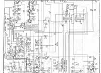
I have a nice Yamaha cr-3020 which I got in for a service, the owner wanted the power board recapped, Output transistors new heat transfer paste, power amp boards recapped, and new bulbs, and all switches cleaned. All above done without issue. The receiver also had very low volume on FM (before all above work also) I have found where the signal is lost. It's fine where R219 joins to R167 and at the other end of R219 the signal is gone.(just under IC104) So if TR135 is turned on, which is probably is as the Base =0.64 (slightly higher on other voltage meter) it would pull the signal to ground I presume, I have tested the following:
R219= 14.7k
Tr135 = hfe212, uF=687mV, B=0.64, C=0V, E=0V
B=0.64, C=0, E=0V
New c171 & c170 even though they tested fine, I had them out for testing so replaced them.
C143=46pF is fine.
I see TR142 and TR141 look like they detect DC on the output possibly?
I have read the following The base on both are B= -11.76, E=0, C=0V
, as far as I can see E & C are expected at 0V and Base should be -10.44 hard to see on diagram
I checked the voltage with relative to ground on D116 (IS1555) and anode end = -11.71 and cathode= -1.52
What voltage should I expect at the cathode? If we expect TR135 should be in off state, then we need a lower voltage on the base? Am I seeing this right? I'm no expert so could do with some advise please?
Attachments
Hi Mooly how are you? Thanks for taking a look.
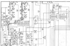
I have attach 2 other screen shots, the resolution is not great, should I be looking at BE coming into the board? or the line going left from VR108 to c166? I can see one voltage marked on the + side of C166 which looks like 13.08 (collector of TR132) i have tested each transistor (most out of circuit) with transistor tester and all seem ok. And quickly tested just the ESR on the electrolytic caps. I wonder if VR108 just needs to be adjusted?
I have attach 2 other screen shots, the resolution is not great, should I be looking at BE coming into the board? or the line going left from VR108 to c166? I can see one voltage marked on the + side of C166 which looks like 13.08 (collector of TR132) i have tested each transistor (most out of circuit) with transistor tester and all seem ok. And quickly tested just the ESR on the electrolytic caps. I wonder if VR108 just needs to be adjusted?
Attachments
Oh just realized VR108 is the an external pot. I have unsoldered it and its reading 17.66k ohms, and it varies ok from 0 to 17.66k ohms on the center tap. The back two pins connected seems to just act as a switch from open to 0 ohms. I presume this is ok the schmatic seems one side is variable and the other wafer a switch?
I'm fine thanks ")
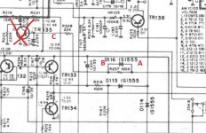
You need to look at the voltage on the anode of D116 which is the common point for all three mute transistors. If that voltage is high then it will be in mute.
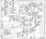
On the right hand side of the first image is a terminal marked 'BE'. It might be an idea to see where that goes to.
Going the other way and the line becomes to faint to make out properly but it seems to go to R211 and maybe even further.
You need to look at the voltage on the anode of D116 which is the common point for all three mute transistors. If that voltage is high then it will be in mute.
On the right hand side of the first image is a terminal marked 'BE'. It might be an idea to see where that goes to.
Going the other way and the line becomes to faint to make out properly but it seems to go to R211 and maybe even further.
Hello friends,
I cannot contribute too much technically here, but the service manual is available on the hifiengine for free (just register).
Regards,
Winfried
I cannot contribute too much technically here, but the service manual is available on the hifiengine for free (just register
).Regards,
Winfried
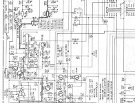
Ok I measured BE and it's -13.2v (or close anyway, lost the piece of paper I wrote it on) I also traced that faded line your on about and it goes to the Collector of TR124, I measured the voltage here and its 13.49V, there are two voltages marked on the collector on the schematic -13.30 and -12.57 any idea why that is? (switch position related?) I confirmed by un-soldering the Switch also and it seems to act ok as a switch on one wafer and a pot on the other so like you said it looks related to the base supply to the 3 mute transistors, as the darker line above it can be turned of with the switch so this is likely unrelated as the issue is there with the switch either on or off. I found the diagram where BE comes from, I will include it. The voltage at D116 from -11.71 to -1.52V is this correct? The diode reads ok with diode tester the resistor in parallel is spot on 100k
Attachments
If the anode volts of D116 is negative 11v approx (lets work with it in that state) then you should have a negative voltage on the base of all three mute transistors and so they should all be OFF or unmuted.
TR135 base volts which I think you mentioned in post #1 as being plus .64 volts should be negative. It is pulled negative via the 100k across the diode.
TR135 base volts which I think you mentioned in post #1 as being plus .64 volts should be negative. It is pulled negative via the 100k across the diode.
Ok thanks, would it be safe to pull the + side of c170 i.e. disconnect TR135 to see if the rest of the circuit is working ok? I know I won't achieve much in doing this, but just to see if everything else is working, since I do not have DC on the output, its probably safe? I might just replace TR141 & TR142 and TR135 also, encase One of them is leaking, Or diode D113 if it's leaking could be pulling the voltage positive maybe? I have put it aside for the moment, have a much easier sansui su2900 to work on first, with the usual noisy c1313 transistors. Thanks for you help so far
Absolutely safe, this is all small signal circuitry and nothing to do with DC offsets and protection and so on.
You could remove all three of those transistors as a test, in fact that might be the best approach as there is then no doubt at all that can be influencing anything.
You could remove all three of those transistors as a test, in fact that might be the best approach as there is then no doubt at all that can be influencing anything.
Ok finally getting back to this, I pulled out c170 and the volume is restored as expected, at least everything else is ok. With c170 removed I measured the following.
TR135 B=675mA, V=5mA and C=5mA.
D116 anode =-12.6V and cathode=-1.7V
TR141 & TR142 both B= -13.2V, C and E are 0V.
According to the schematic I should have -10.44V at the anode not -12.6V.
So where to go from here? replace TR135 (2sc1918 -- NPN) and switching diode D116 (IS1555) with an IN4148 Or if anyone has any other suggestions?
Last edited:
With TR135 removed you should have the same voltage on each side of the diode D116 because of the parallel 100k. C171 would be suspect in this case because nothing else is shown connected to that line.
If there is negative 10 volts (approx) on C171 then the transistor would be suspect.
If there is negative 10 volts (approx) on C171 then the transistor would be suspect.
Ok I did what you suggested Mooly, I de-soldered TR135 and this is the voltage reading with reference to ground. D116 is -11.92v at anode and 3.05V at cathode.
C171 on negative side 0v and positive side similar 5mV. Just to speed things up a little I have replaced both TR135 With ksc1845 and the diode D116, also made sure the cap C171 was the right way around and reads ok (new cap). So still getting 0.67V on the base of TR135. So I should probably de-solder TR135 and aim to get -11.92 on D116 both sides, maybe by disconnecting the other two muting transistors on this line? We also have the option to just leave c170 disconnected but then the muting pot. will not work
C171 on negative side 0v and positive side similar 5mV. Just to speed things up a little I have replaced both TR135 With ksc1845 and the diode D116, also made sure the cap C171 was the right way around and reads ok (new cap). So still getting 0.67V on the base of TR135. So I should probably de-solder TR135 and aim to get -11.92 on D116 both sides, maybe by disconnecting the other two muting transistors on this line? We also have the option to just leave c170 disconnected but then the muting pot. will not work
Look at the circuit. With the transistor removed points A, B and C should all be equal. If they are not then either something is dragging the voltage down or the diagram is wrong.
Is C171 fitted correctly? Looks like positive should go to ground.
Is C171 fitted correctly? Looks like positive should go to ground.
Attachments
Hi, I replaced TR135, TR141 and TR142(1845 transistor) and C171, D116, and still the same. Yes I confirmed that c171 is the right value and the right way around with positive going to ground.
So at the moment I have TR135 Fully removed, C170 one leg lifted, Both the bases from TR141 and TR142 Lifted. D116 replaced and R257 was already tested out of circuit and was spot on 100k. I also replaced C168 right way around, and confirmed that the negative side (also BE) is -13V, which is what is expected approx. (BE should be -12V and RE = +12V) I checked both are ok coming into the circuit board
Still getting -13V at the anode of D116 and about 2.8 to 3.5V on the cathode depending on position of the muting pot. Maybe the resistor in parallel with D116 is testing fine but not working under load. Getting there, but this one has proven to be a right pain
Just a update, I decided to remove R228 and now I have -11.9V on the cathode of D116, strange on the circuit diagram it does not show R228 going anywhere else, but in fact its going to one of the pins on SW101(rec cal, dx fm auto dx switch) , the only other place it goes is the base of TR135 which is removed. I will upload a picture of the component layout in a few mins.
- Status
- This old topic is closed. If you want to reopen this topic, contact a moderator using the "Report Post" button.
- Home
- Amplifiers
- Solid State
- Yamaha cr-3020