I think knutn is trying to say that if the dominant pole is the output capacitance then more capacitance just makes it more dominant. But, or course, that's a plan that doesn't work well at all. For one reason, real capacitors large enough to create a dominant pole on the output has a self resonance, due to its inductance, that is below the 0dB loop gain frequency. The classic VAS Miller cap works because the self resonance of a ~100pF cap is very high and it is small and can be connected to the VAS transistor with very short wires/traces.
Capacitor Self-resonant Frequency and Signal Integrity | Advanced PCB Design Blog | Cadence
Another reason is that making the naturally dominant pole more dominant gives the best bandwidth vs creating another pole that is so low that it dominates the natural pole of the VAS. Even if the output is the VAS, the naturally dominant pole is the Cbc and not the collector loading.
Last edited:
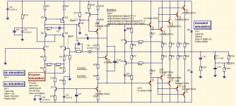
Before anyone asks: Yes, it is a modified (20 W) Hiraga. More details can be found at: Class A Audio Power Amplifier Mimir
I'll try to explain why I think it is better with a common emitter output stage.
A 'better' example might backup you up. A slow design with significant distortion would not be 'better' in many people's view.
I am working on building up Michael Chua's C300 amplifier which does include a Zobel load on it. I have a SPICE simulation of it going. I am trying to figure out what could go wrong with it through simulation. I have been able to put 10 to 20 nF on it without problems, but once 100 nF is directly loaded on it, oscillations start. I can increase the Miller compensation capacitor to bring the pole down to be stable, but if the loop bandwidth is reduced too much, THD increases. It seems to be in the neighborhood of 0.05% to 0.1% for 20 kHz @ 200 W output to an 8 ohm load (at least in simulation).
Why are you using MJE340 and MJE350 in your Vas - the datasheets don't give any clue as to the fT which makes them unsuited to this application.
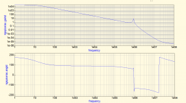
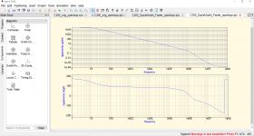
Ok, to get a better handle on the performance, I did SPICE analysis and repeated the analysis of Bonsai in this presentation to check my work:
Output L_1
The first set of plots is a sanity check to show that the simulation of the circuit from the presentation recapitulates the Bode plot results, and it appears to do so.
The second set of plots is the circuit I have been testing with a 33 pF Miller compensation feedback and MJE340/350 transistors as the VAS and Darlington drivers. The phase margin appears to be about 60 to 70 degrees.
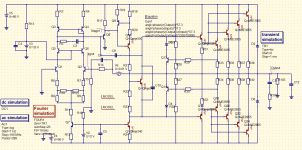
The third set of plots is the circuit with a 100 pF Miller compensation feedback network and MJ15032/33 transistors as the VAS and Darlington drivers with 0.01 uF load and 1 uH series inductance output. The phase margin appears to be about 50 to 60 degrees.
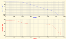
The fourth set is the circuit with the 100 pF Miller compensation feedback network and MJ10532/33 transistors with a 0.1 uF load and 0 uH series inductance output, showing the appearance of the pole due to the capacitance on the output.
I think this might help explain some of the issues here, that the output is not unconditionally stable and probably needs the output inductor, though I think for the MJE10532/33 design 0.03 to 0.04 uF of capacitance can be tolerated before oscillations become possible.
Output L_1
The first set of plots is a sanity check to show that the simulation of the circuit from the presentation recapitulates the Bode plot results, and it appears to do so.
The second set of plots is the circuit I have been testing with a 33 pF Miller compensation feedback and MJE340/350 transistors as the VAS and Darlington drivers. The phase margin appears to be about 60 to 70 degrees.
The third set of plots is the circuit with a 100 pF Miller compensation feedback network and MJ15032/33 transistors as the VAS and Darlington drivers with 0.01 uF load and 1 uH series inductance output. The phase margin appears to be about 50 to 60 degrees.
The fourth set is the circuit with the 100 pF Miller compensation feedback network and MJ10532/33 transistors with a 0.1 uF load and 0 uH series inductance output, showing the appearance of the pole due to the capacitance on the output.
I think this might help explain some of the issues here, that the output is not unconditionally stable and probably needs the output inductor, though I think for the MJE10532/33 design 0.03 to 0.04 uF of capacitance can be tolerated before oscillations become possible.
Attachments
-
Qucs-S-files.zip11.4 KB · Views: 44
-
 C300_MJE15032_BodePlot_Capacitively_Loaded.png84.3 KB · Views: 85
 -
 C300_MJE15032_Schematic_Capacitively_Loaded.png76.2 KB · Views: 83
 -
 C300_MJE15032_BodePlot.png85.9 KB · Views: 84
 -
 C300_MJE15032_Schematic.png75.7 KB · Views: 78
 -
 C300_MJE340350_BodePlot.png100 KB · Views: 179
 -
 C300_MJE340350_Schematic.png76.3 KB · Views: 184
 -
 SimpleAmp_BodePlot.png78 KB · Views: 183
 -
 SimpleAmp_Schematic.png59.9 KB · Views: 209
Your right Mjona online I cant find the Ft but in one equivalent book I have says --equivalent is BD232 which is 3MHz but in my Mullard equivalent book their higher spec one has the BD232 as a line driver in TV,s at 20MHz but I suspect its the lower spec =3MHz Ft as all the other ones near that year of manufacture have 3MHz .
There are different versions of the MJE340 .
There are different versions of the MJE340 .
Ok, to get a better handle on the performance, I did SPICE analysis and repeated the analysis of Bonsai in this presentation to check my work:
Output L_1
The first set of plots is a sanity check to show that the simulation of the circuit from the presentation recapitulates the Bode plot results, and it appears to do so.
The second set of plots is the circuit I have been testing with a 33 pF Miller compensation feedback and MJE340/350 transistors as the VAS and Darlington drivers. The phase margin appears to be about 60 to 70 degrees.
The third set of plots is the circuit with a 100 pF Miller compensation feedback network and MJ15032/33 transistors as the VAS and Darlington drivers with 0.01 uF load and 1 uH series inductance output. The phase margin appears to be about 50 to 60 degrees.
The fourth set is the circuit with the 100 pF Miller compensation feedback network and MJ10532/33 transistors with a 0.1 uF load and 0 uH series inductance output, showing the appearance of the pole due to the capacitance on the output.
I think this might help explain some of the issues here, that the output is not unconditionally stable and probably needs the output inductor, though I think for the MJE10532/33 design 0.03 to 0.04 uF of capacitance can be tolerated before oscillations become possible.
Forgetting questions about inductors etc for now 2SA1381 is a better choice for the Vas position because this extends the unity gain bandwidth.
Bonsai has mentioned the rate of decline in gain of 20dB/decade with compensation which is equivalent to an angle of 45 degrees starting from the point where the gain reaches - 3dB (0.707).
If you go with 2SA1381 the -3dB frequency will increase and the point where the phase angle starts to change will also increase - this is around a decade in frequency below the new -3dB point.
The decade rule also applies to compensation in that the Vas pole has should be ten times greater than any other pole to be dominant.
C6 has been mentioned in a different context in a previous post. Bob Cordell has cautioned against using lead capacitors. This could also compromise the dominance of the Vas compensation.
Before anyone asks: Yes, it is a modified (20 W) Hiraga. More details can be found at: Class A Audio Power Amplifier Mimir
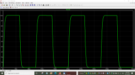
As far as I can tell from a 10kHz square wave test -peak voltage of 10 into 8R with 4uF in parallel, there is no need for any compensation capacitors provided there is a buffer resistor of 0R22 between the output and the load and there is a low pass filter on the output -adding 1n2 in parallel with R2.
The shape of the square wave shown below improves if the 4uF is removed.
Attachments
10nF parallel with 8R square wave 10kHz
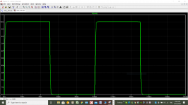
The result is below. In this I changed the output transistors to MJL21193 and MJL21194 from MJL3281 and MJL1302 I used for the previous image. Hiraga used 2SB and 2SB prefix devices in his original design.
I also reduced the added capacitor to make a low pass input filter from 1n2 to 680p. The time base is also reduced for a closer inspection in the image.
The output buffer transistor of 0R22 makes a material difference. This is a strategy seen in Naim amplifiers and also seen in many Linsley-Hood designs.
When I get some time I will look at a Tian test to see what the stability margins are with both sets of output devices.
Attachments
Maybe I am missing something. Seems to need compensation for capacitive loads even with 0.22R
Regardless, an EF driver design can achieve unconditional stability and still drive ultrasonic frequencies. The Hiraga is a good design in terms of bang-for-buck simplicity, but for me, no sale. EF/CE is not worth arguing. There is the hybrid EF-CE as well.
Getting rid of the inductor
Boiling it down to two parameters, unity loop gain needs to be around 600KHz max and phase margin greater than 90 degrees. The OP design has too much bandwidth in my view.
I followed the link knutn provided in post 43 which has a further link to a previous Hiraga variant he had built Class A Audio Power Amplifier Mimir so I believe he is for real regardless of the simulation he posted and what anyone might take from it.
Anyway I am attaching the simulation for square wave test I did. Adding 4uF in parallel with 8R could be looked at as abuse so I have moderated the load for a variety of capacitance values from 5nF to 2uF.
Even with 30MHz unity gain output devices these would be the lowest rated in the circuit on that score, so it appears that not unlike the JLH simple Class A circuit these would set the dominant pole, and, do so at the end of the conduction chain where there is a high damping factor.
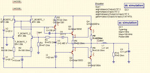
I have increased the value for R7 to adjust the dc offset. There is a directive for temperature of 27 degrees C I think the amplifier will run hotter than that but I left that unchanged.
Anyway I am attaching the simulation for square wave test I did. Adding 4uF in parallel with 8R could be looked at as abuse so I have moderated the load for a variety of capacitance values from 5nF to 2uF.
Even with 30MHz unity gain output devices these would be the lowest rated in the circuit on that score, so it appears that not unlike the JLH simple Class A circuit these would set the dominant pole, and, do so at the end of the conduction chain where there is a high damping factor.
I have increased the value for R7 to adjust the dc offset. There is a directive for temperature of 27 degrees C I think the amplifier will run hotter than that but I left that unchanged.
Attachments
Last edited:
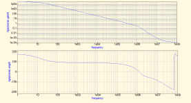
Thank you for your contribution. However, the point with my modification of the original Hiraga, was to reduce the ouput impedance to better suite my loadspeakers. And an added series resistance then is not an option. Instead, the amplifier is stabilized by the two 68pF capacitors (C26,27) (post #42). This gives an open loop bandwidth of about 60 kHz with pure resistive loading. With a capacitive load of 1 uF, this drops to about 15 kHz (simulation).
I don't get your values. According to my simulations, the phase margin at 20 db closed loop gain is about 80 degrees. And, you are right, I have never seen any signs of oscillations with the two 68 pF Miller capacitors.
You are looking at the gain of the feedback loop here. It needs to be made to decline so it reaches 0 dB before the phase angle reaches -180 degrees.
The x and y axes in your .raw file have been altered and the 0dB gain level is not on the chart.
N101N has commented about BD139 for which Cordell's .models were used. It is possible that there have been some changes in production over time behind this so I tried some alternatives which need the extra collector to base capacitance.
- Status
- This old topic is closed. If you want to reopen this topic, contact a moderator using the "Report Post" button.
- Home
- Amplifiers
- Solid State
- Stability of an amplifier under capacitive loading