Yes both channels.
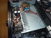
I don't believe this amplifier was ever touched before do the amount of lint inside and the other thing is the trim pots are almost maxed out like they where in the other one I bought a couple of months ago.
Already ordered some new resistors (300/330/360/390 ohms) to replace the 470 ohm one in the circuit so I can have a bit more range on the trim pot.
Going to play with the pre amp section to see what is going on.
PS: had it playing yesterday for a few hours and it never warmed up, nothing just stone could.
Good find, 'glad that mystery is solved. So it was a bad switch that caused the bias to zero out? That's all the more reason to trace out the circuit of the amplifier stage to learn how not to design its biasing circuit. As many of us here feel they should play with anything adjustable, I think that would be useful to know.
The faulty switch was causing the right channel to drop out (very low level) if "normal" was selected but it would be fine in "Direct" mode.
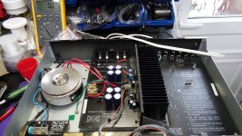
Checked power amp board and the board never has been repaired before everything is original but can't adjust the bias because trim pot almost maxed out.
Checked power amp board and the board never has been repaired before everything is original but can't adjust the bias because trim pot almost maxed out.
As there is no schematic or full description of the amplifier available, it's unlikely anyone following the thread has more than a general idea of the first version A1 amplifier design you are referring to.
It would allow some understanding if you sketched one of the power amplifier circuits including the mode switch and associated signal grounding arrangement. However rough it may appear, post it here. We aren't all da Vincis and don't need pro. standard graphics to follow circuits or sections thereof. It's understandable that you may not have a suitable mobile phone, digital camera or the inclination to do this but there are simple and free software drafting programs, if need be.
It would allow some understanding if you sketched one of the power amplifier circuits including the mode switch and associated signal grounding arrangement. However rough it may appear, post it here. We aren't all da Vincis and don't need pro. standard graphics to follow circuits or sections thereof. It's understandable that you may not have a suitable mobile phone, digital camera or the inclination to do this but there are simple and free software drafting programs, if need be.
Hi Ian (?)
I see where you coming but the amp is repaired and put back together and I really don't want to take it apart again, unfortunately there is no easy access to the power amp from under the case everything has to be done from the top even the speaker terminals have to be remove to get the board out.
Maybe in the next one...
OK, that's fine if you are satisfied and bias remains reasonably stable after a workout with a dummy load. As I understand it, you settled on 10mA bias current which suggests it's most likely a CFP output stage design, otherwise it wouldn't sound so good, particularly not at the original settings.
If we change factory bias settings significantly, it makes sense to test them over the full range of operation because we don't find thermal issues at modest output levels with the case open on the bench - i.e. the way average DIYs do their sanity checks. That doesn't prove much that will save the amp as it becomes stretched toward some new safe limit when, for example, it's located in a hifi cabinet or close-fit shelving.
If we change factory bias settings significantly, it makes sense to test them over the full range of operation because we don't find thermal issues at modest output levels with the case open on the bench - i.e. the way average DIYs do their sanity checks. That doesn't prove much that will save the amp as it becomes stretched toward some new safe limit when, for example, it's located in a hifi cabinet or close-fit shelving.
Actually I settled at 15mV at the 0.22R resistor so 68mA if my math doesn't fail me.
I always put the repaired amplifiers on test for a few days with the cover on.
The 2 A1 mk1 that I fixed recently don't get hot, even after 3 or 4 hours playing temp is around 32C at the body of the transistors.
I always put the repaired amplifiers on test for a few days with the cover on.
The 2 A1 mk1 that I fixed recently don't get hot, even after 3 or 4 hours playing temp is around 32C at the body of the transistors.
Hi rs232 kindly linked me to post hoping I can get some help on the mk1, right channel is badly distorted the right channel bias on the bd139 is the full supply of 1.1v with .56v bias on left channel(1.1v full supply) the right channel ifeal emmitter voltage is about 20mv with left channel about 5mv. Iassumed right bd139 was open base but after removing it tests fine on a transistor checker. I can't find any other issue the output transistors seem to measure fine , and I can't find any discrepancies in component value thanks in advance antony
The image in post #5 isn't the model A1 with TDA1514 - go to the schematic in the attachment.Hello so i bought a cambridge a1 mk1 (the original version) off someone and they said that the main board glass fuse blew and to change it and it would work. However after changing it the amp still doesn't turn on.
None of the other fuses had blown, it was the T3.15A which blew which is the last fuses. I also read a few youtube comments which said it could be the transformer since none of the first fuses blew.
Can anyone help me?
I have a DMM so can test things if needed be.
This is the model "Atac 3" released in 1995 - go to
Cambridge Audio Atac3 | Hifi-Wiki
For me one of the best sounded integrated amplifier in the economy class.
From this amp I have the service manual - unfortunately on paper and not as PDF and only in low resolution.
The Phono-RIAA amp MM module (available as upgrade kit) was very close to the RIAA devices from Creek (OBH-series). The most interesting feature is an approach with a SRPP stage realized with BjT (small signal versions in a TO-92 outline). RIAA Schematic is identical to those phono preamp from A3i - go to
https://www.diyaudio.com/archive/bl...-modded-cambridge-audio-a3i-a3i-schematic.pdf
Attachments
To tiefbassuebertr the amp is question is the original A1 also known as A1 mk1 and is a full discrete components audio amplifier (no integrated stuff anywhere).
There are 3 different versions of this amplifier.
1st one is the original one described above
2nd one has a E I transformer and a LM4765
3rd one has a toroid transformer and is based on the TDA1514.
None of them share the preamp board/design.
To Antspants check associated resistors and trimer as this last one can "dig" a hole in the track inside it and give strange readings.
PS: Don't forget that the BD139 is mounted with face to heatsink.
Pictures of 2 different version os the A1 will post pic tomorrow for the MK1
Attachments
Last edited:
VBE multiplier circuit: Q611 (BD139), C611 (100nf), R620 (470r), R621 (1K5) and P601 (470r).
If everything reads rights reset idle current (compre with good channel) and test if noise/distortion is still there.
If it is still there disconnect the preamp board (had several issues with it) and test again.
Repaired 2 different A1 mk1 with sound issues caused by the preamp board.
If everything reads rights reset idle current (compre with good channel) and test if noise/distortion is still there.
If it is still there disconnect the preamp board (had several issues with it) and test again.
Repaired 2 different A1 mk1 with sound issues caused by the preamp board.
Last edited:
Welcome to the "oops" club. Using plain and slippery meter probes? If so, get yourself some hook probes or fit some cheap IC clips to probe leads before trying to manage both probes and adjust a loose meter (or some similarly awkward operation) at the same time. Fortunately, the output transistors are about the cheapest genuine spec. power transistors anywhere.
Hi there thanks for all the advice had a disaster today and shorted output transistor! Will report more fully tomorrow
There is an image in post 155 which shows an insulating washer to isolate screw securing the tab of the BD139 to the heat sink. Without this you are reliant of the paint for isolating the collector from other parts of the amplifier - possibly shorting to earth and similarly the base of the TIP3055.
Hi I must say a big thanks to everyone all the replies have been really helpful . I'm much more au fait with valve technology having repaired and modded mainly guitar and bass kit for over 40 years and had 2 years of tutorials from a ex senior Marshall designer, never really got into these ew fangled sid state stuff except for relatively simple pedals and amp stuff! Stereo stuff is way more complicated and without a circuit diagram I'm fighting a loosing battle. Brief recap as I might have one more go, right channel very distorted, full vbe multiplier supply of 1.1v on base of bd139, 30mv on output transistors left channel 1.1v supply with vtage drop to 5.9v on base of bd139 and around 10mv on emitters of output transistors .Assumed open base on left hand bd139 replaced it in correct orientation now had 0.88v instead of 1.1v and still full supply voltage of .88v on bd139 base checked both associated transistors which both have 32v on collector but only 0.4v on bases and 0.88v on emitters, right channel was still OK with 0.6v on bases and 1.1v on emitters. Double checking readings is when I shorted q313 both channel supply rail fuses blew q313 and both left hand channel output transistors
Blew. As I hadn't sorted vbe multiplier issues and couldn't find any other problems I'm not
convinced its worth pursuing any
Further without a circuit diagram although I don't like been defeated and I've only ly failed once to repair a bass amp with loads of smd in it, vile stuff especially when manufacturers refusing g to supply diagrams and parts anyway thanks again will let you know what I end up doing if not proceeding the amp or parts will free to a good home for postage cost
- Home
- Amplifiers
- Solid State
- Cambridge audio a1 mk1 not powering on.