I suppose it's possible you might have zapped the muting/switching transistors at the input.
You should check R358 which is a 100 ohm/1 watt.
Q429, 430 and 431 also need checking. You could actually remove those as a test and see if the amp works.
But we are jumping ahead... although the above are worth a look first given what happened with the reversed plugs and the fact no obvious damage seems to have occurred in the output stage.
I suppose it's possible you might have zapped the muting/switching transistors at the input.
You should check R358 which is a 100 ohm/1 watt.
Q429, 430 and 431 also need checking. You could actually remove those as a test and see if the amp works.
But we are jumping ahead... although the above are worth a look first given what happened with the reversed plugs and the fact no obvious damage seems to have occurred in the output stage.
Great - will investigate those now
")
You should check R358 which is a 100 ohm/1 watt.
Q429, 430 and 431 also need checking. You could actually remove those as a test and see if the amp works.
R358 on the right board checked out to be 98.5 ohms.
Q431 - 2SC2878 NPN - working, no shorts.
Q430 - 2SC1775 NPN - working, no shorts.
Q429 - 2SA872 PNP - working no shorts.
Tried running before I soldered them back in but alas, still no sound.
There is quite a loud hum/buzz in the left speaker when I touch the left board around CZ301 or the components close to it.
The buzz will be normal as it sounds like it is just picking up stray 'hum' from you as you touch around that area.
It was worth trying those transistor... but it now looks like we are down to normal fault-finding.
I would begin by checking the basics.
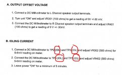
1/ That DC offset is below -/+50 millivolts as measured at the junction of R456/457 which seems to be test point 5 on the board.
2/ Check the bias current by measuring the voltage between TP6 and TP7. It should be around 5 millivolts, so very a low value.
You can compare readings with the good channel.
Those 2 checks tell us much about the state of play of the output stage.
It was worth trying those transistor... but it now looks like we are down to normal fault-finding.
I would begin by checking the basics.
1/ That DC offset is below -/+50 millivolts as measured at the junction of R456/457 which seems to be test point 5 on the board.
2/ Check the bias current by measuring the voltage between TP6 and TP7. It should be around 5 millivolts, so very a low value.
You can compare readings with the good channel.
Those 2 checks tell us much about the state of play of the output stage.
1/ That DC offset is below -/+50 millivolts as measured at the junction of R456/457 which seems to be test point 5 on the board.
2/ Check the bias current by measuring the voltage between TP6 and TP7. It should be around 5 millivolts, so very a low value.
I must be missing something - I can see the test points on the schematic but I don't find them on the actual board.
I've worked on Synthesizers before where the test points are to be found on the board, clearly labelled, is it not the case with amplifiers?
I tried to get the measurement between R456/457 by connecting probe to GND and the other to the little jumper wire that connects the two resistors (the big white square ones). It read 70+ mV!
I tried the same place on the Left board and it was also 70+ mV.
I noticed the right side was getting very hot! The left side was cold but something on the right side was getting way too toasty! I shut it off.
Then I moved to the working amp to make a comparison - this is where woe turned quickly to despair...
I checked the right side in the same place - approx 10 mV here. Then I went to do the same to the left side....booom


I saw sparks and the smell...I guess the probe must have shorted something. Now I broke the new amps left channel - I could cry
I swapped in the left channel from the old amp and I at least have 1 working unit.
But now I have multiple problems to find and fix...I'm having terrible luck with this.
Mooly, i'd be more than happy to send you a couple hundred pounds if you could continue to assist me on this. I'm more determined than ever to redeem this situation. Of course I understand if you don't have time.
I tried the same place on the Left board and it was also 70+ mV.
I noticed the right side was getting very hot! The left side was cold but something on the right side was getting way too toasty! I shut it off.
Then I moved to the working amp to make a comparison - this is where woe turned quickly to despair...
I checked the right side in the same place - approx 10 mV here. Then I went to do the same to the left side....booom
I saw sparks and the smell...I guess the probe must have shorted something. Now I broke the new amps left channel - I could cry
I swapped in the left channel from the old amp and I at least have 1 working unit.
But now I have multiple problems to find and fix...I'm having terrible luck with this.
Mooly, i'd be more than happy to send you a couple hundred pounds if you could continue to assist me on this. I'm more determined than ever to redeem this situation. Of course I understand if you don't have time.
Oh dear
OK, so I can give you all the help needed via the forum, that isn't a problem (and no money required... but thanks ) but you have to be realistic... is this going to be beyond your abilities now?
I'm sure if you check around the output stage and those 0.2 and 0.05 ohm resistors you will find some evidence of failures. Quite possible also Q417/418.
If you can locate on the circuit the two points you shorted it could in narrowing down what will have failed.
OK, so I can give you all the help needed via the forum, that isn't a problem
(and no money required... but thanks ) but you have to be realistic... is this going to be beyond your abilities now?I'm sure if you check around the output stage and those 0.2 and 0.05 ohm resistors you will find some evidence of failures. Quite possible also Q417/418.
If you can locate on the circuit the two points you shorted it could in narrowing down what will have failed.
A word of caution with these NAD amps, unless it's already been mentioned; the electrolytic capacitors used on these aren't too great. By this age, many of the capacitors are probably not doing so well. A quick check of ESR usually bears it out, although the last few dozen older NAD amps I've seen had capacitors SO bad I've just begun replacing every electrolytic as a matter of course.
My last C370 had failed completely due to nothing more than capacitors. The infamous little board with the Zener diode was still working! I redid it for longevity's sake anyhow.
My last C370 had failed completely due to nothing more than capacitors. The infamous little board with the Zener diode was still working! I redid it for longevity's sake anyhow.
Oh dear
OK, so I can give you all the help needed via the forum, that isn't a problem
abilities!? I fear you've been misled

Really can't thank you enough for the help - are you sure I can't offer you something for the trouble?
I'm sure if you check around the output stage and those 0.2 and 0.05 ohm resistors you will find some evidence of failures. Quite possible also Q417/418.
Is this in relation to the original issue or the most recent fiasco? Q417/418 are on the right side and it's the left I just futzed.
If you can locate on the circuit the two points you shorted it could in narrowing down what will have failed.
Pretty sure it must have been the other little bar that runs parallel to the one I was probing. This would have caused a short between the -V64 pin which is also connected to the ouptut transistors Q328/324/322 amongst other things.
Last edited:
A word of caution with these NAD amps, unless it's already been mentioned; the electrolytic capacitors used on these aren't too great. By this age, many of the capacitors are probably not doing so well. A quick check of ESR usually bears it out, although the last few dozen older NAD amps I've seen had capacitors SO bad I've just begun replacing every electrolytic as a matter of course.
My last C370 had failed completely due to nothing more than capacitors. The infamous little board with the Zener diode was still working! I redid it for longevity's sake anyhow.
Yes, i'm sure that's correct and a recap is on the list
Is this in relation to the original issue or the most recent fiasco? Q417/418 are on the right side and it's the left I just futzed.
That's just me looking at the wrong channel... so you want to check the driver transistors on the other channel.
So it sounds like you shorted the output line to the negative rail.
Do any of the output transistors or those drivers now read short circuit from collector to emitter?
That's just me looking at the wrong channel... so you want to check the driver transistors on the other channel.
So it sounds like you shorted the output line to the negative rail.
Do any of the output transistors or those drivers now read short circuit from collector to emitter?
Output transistors:
Q321 and Q327 (2SA1943 PNP) both have continuity across B and C.
Q323 (2SA1943 PNP) has continuity across B, C and E.
Driver transistors:
Q317 (2SD669A NPN) has continuity across B, C and E.
Q318 (2SB649A PNP) has continuity across C and E.
You will read various 'parasitics' from other components connected around these parts if you test in circuit. What we are looking for is catastrophic damage which would show as a short circuit or very very low ohms across the junctions.
If any devices read like that then they are frazzled.
These are all just quick and dirty tests although very useful for getting an initial feel of what damage has occured.
If any devices read like that then they are frazzled.
These are all just quick and dirty tests although very useful for getting an initial feel of what damage has occured.
You will read various 'parasitics' from other components connected around these parts if you test in circuit. What we are looking for is catastrophic damage which would show as a short circuit or very very low ohms across the junctions.
If any devices read like that then they are frazzled.
These are all just quick and dirty tests although very useful for getting an initial feel of what damage has occured.
When you say `in circuit` I take it that you mean whilst soldered in place but not with any power going through right?
I'm also curious about those test points - they are not actual points on the board are they? Some boards do have test points which are labelled as such on the board as well as the schematic.
Soldered in = in circuit. Shorts will always show as a short and also any low value resistors that read high in value or open circuit are detectable.
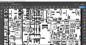
The test points are listed (centre of first image) The IDL ones are just for measuring the voltage across the low value resistors in the output stage and from that result the current can be calculated.
The test points are listed (centre of first image)
The IDL ones are just for measuring the voltage across the low value resistors in the output stage and from that result the current can be calculated.Attachments
Soldered in = in circuit. Shorts will always show as a short and also any low value resistors that read high in value or open circuit are detectable.
The test points are listed (centre of first image)
Ahaaa! Right - there they are
So earlier, when I wanted to test the voltage between 50 millivolts between R456/457 I should have connected one probe to CEN and one to GND as shown below?

You would measure between TP6 and TP7 which are both marked IDL (will be short for idle current).
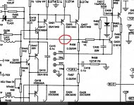
The circuit is missing a 'blob' as shown.
CEN will be short for centre or centre point and is the main speaker feed output. That point would be used for measuring the DC offset. If there is a DC offset fault the relay would not connect the speaker terminals and so you wouldn't know there was a problem (beside noticing the relay didn't operate) if the voltage at the terminals was zero.
GND would be the reference point for the offset measurement.
Attachments
You would measure between TP6 and TP7 which are both marked IDL (will be short for idle current).
Hmm, you seemed to say it was TP5 earlier to check the junction between those two resistors - but it was actually TP6/7?
I would begin by checking the basics.
1/ That DC offset is below -/+50 millivolts as measured at the junction of R456/457 which seems to be test point 5 on the board.
TP5 is to measure the DC offset which ideally should be zero. That is always measured with respect to ground. Any DC offset appears directly across the speaker which is always a bad thing as it causes DC current to flow in the speaker. If the voltage is high (a fault) then the speaker is in danger of being burned out.
TP5 is the main amplifier output point that would drive the speaker.
TP6 and TP7 straddle R456 and R457. The voltage across these points (not measured to ground) indicates the static bias current flowing in the output transistors.
Those two separate tests show much about the operating conditions of the amplifier.
TP5 is to measure the DC offset which ideally should be zero. That is always measured with respect to ground. Any DC offset appears directly across the speaker which is always a bad thing as it causes DC current to flow in the speaker. If the voltage is high (a fault) then the speaker is in danger of being burned out.
TP5 is the main amplifier output point that would drive the speaker.
TP6 and TP7 straddle R456 and R457. The voltage across these points (not measured to ground) indicates the static bias current flowing in the output transistors.
Those two separate tests show much about the operating conditions of the amplifier.
Great, that makes sense - thanks for the explanation
I have worked my way through all the components on the left channel looking for opens/shorts and any resistors that are significantly out of spec. Luckily I have the working left channel to make comparisons. Finding quite a few bits that need replacing - all marked here in red...

Here are the failed bits on the schematic...

Here are the parts so far:
LEFT POWER AMP BOARD:
Transistors:
Q321/327/323 (2SA1943 PNP)
Q317 (2SD669A NPN)
Q318 (2SB649A PNP)
Q315 (KSC2690)
Q316 (2SA1015)
ICs:
3IC1/3IC2 (TL431) Regulator
Resistors:
R370/354/352 0.2/1W 5% Fusible
R348 75/0.5W 5% Metal Oxide Film
R344 2K2/3W 5% Metal Oxide Film
R337 100/1W 5% Fusible
R341 330/0.5W 5% Metal Oxide Film
Capacitors:
C306 2200uF /6.3V 85C
With any luck might replacing these fix the damage caused by my little probe accident - or is that simply wishful thinking?
Most of the time anything shorted would produce a constant beeping noise when testing with the DM (continuity mode) - but there were a couple of points where it would beep just once and then stop! It would beep only a single short time each time I retested that point- what could this indicate?
Last edited:
- Status
- This old topic is closed. If you want to reopen this topic, contact a moderator using the "Report Post" button.
- Home
- Amplifiers
- Solid State
- A sorry tale of woe and stupidity: NAD C370