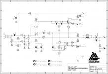
Hello Bogdan,
Here is something I made quickly.
let me know if you have any suggestions for component wattage and layout.
regards
prasi
Hi prasi, great you are quick
") On a first look I don`t see any problems, but may be few minor changes in the schematic it`s stil a prototype and I`m open to suggestions..
On a first look I don`t see any problems, but may be few minor changes in the schematic it`s stil a prototype and I`m open to suggestions..Hi, ok thank you
Did you measure with higher bias current and/or with higher output levels?
What would you suggest in order to achieve higher output power, doubling BJT´s and MOSFETS?
This isnt too easy, as i see it, as you want to see current in both of them and you want to use emitter/source resistors for both of them in order to spread the load evenly
I love it - this is a very nice looking amplifier schematic. I was surprised by the two pole compensation around one device - in that I've found in simulations that it's been necessary to use a compound (two device) VAS to be needed for full benefit from two-pole taken around it - but simulations is not an actual build which you have done.
I did detailed simulations few months ago, so I don`t remember quite well, but the solution is "simulation driven". I could try the difference, C61 to output bjt emitter?
Hi, ok thank you
Did you measure with higher bias current and/or with higher output levels?
What would you suggest in order to achieve higher output power, doubling BJT´s and MOSFETS?
This isnt too easy, as i see it, as you want to see current in both of them and you want to use emitter/source resistors for both of them in order to spread the load evenly
I`m not considering larger power it`s a small class A amp for home use and efficient speakers.
I`m more interested in suggestions for different operating points and compensation that could be better than like it is right now. I allready tried some things..
Hi, I understand
I just think it could be of interest for those with not-so-efficient speakers
You suggest 1.5A bias current, right? Did you measure with this?
Not yet, next I will do the measurements with 4 ohm load and higher bias points.
Hi, I understand
I just think it could be of interest for those with not-so-efficient speakers
You suggest 1.5A bias current, right? Did you measure with this?
Not yet, next I will do the measurements with 4 ohm load and higher bias points.
Member
Joined 2009
Paid Member
Thanks Bigun, Mr. Triatic and Bogdan,
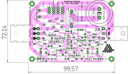
yes, I understand its a prototype. If a "Fearless Amp Builder" wants to try it out, here is an improved one, with plenty of options for components.
regards
prasi
Prasi, great this version looks much better.
There are 2 controls I`m gonna put on my version that could be useful and you could place 2 pin connectors on a pcb as a option.
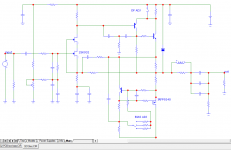
First is to adjust the bias current with 3-4 position, rotary switch and second is toggle switch for bypassing degeneration resistor and changing damping factor. See the attached schematic for example.
Cheers.
Attachments
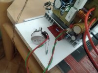
On the proto, I'm changing bias with a pot it's on wire, not shielded and there is no problem, cable it's not sensitive to any kind of noise. I think it's a good idea to have these controls on front panel to play with different sound characters and performance points to suit wider range of speakers..
Btw, any ideas for lowering 3rd harmonic?
Tonight I will send data for differences in distortion between BD140, BF872 and KSA1220 and 4 ohm load measurements on higher bias at full power.
Btw, any ideas for lowering 3rd harmonic?
Tonight I will send data for differences in distortion between BD140, BF872 and KSA1220 and 4 ohm load measurements on higher bias at full power.
Attachments
Last edited:
Member
Joined 2009
Paid Member
Prasi, great this version looks much better.
There are 2 controls I`m gonna put on my version that could be useful and you could place 2 pin connectors on a pcb as a option.
First is to adjust the bias current with 3-4 position, rotary switch and second is toggle switch for bypassing degeneration resistor and changing damping factor. See the attached schematic for example.
Cheers.
will bypassing the degeneration impact the compensation requirements ?
Member
Joined 2009
Paid Member
Btw C13, output cap if it`s on pcb, it will consume lot of space, plus bypass caps..10mF for 8 Ohm speakers it`s an minimum imo. I`ve made separate pcb for ouput caps bank. As you wish this is just my opinion.
Perhaps there’s nothing wrong with the simple 1+1 output cap but it means having this big can on there and I agree, aesthetically it’s ugly on the small pcb. One option is a chassis mounted cap. Another option is a collection of medium sized caps in parallel. Vladimirk made a separate pcb with a circle of caps; he had some interesting comments on this:
Rails Decoupled SE Amplifier
Yes Bigun, I agree with Vladimir`s observations..
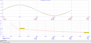
First, simulation distortion results, for later comparing, with 4 Ohms load, 1.45A idle current, about 25W peak or about 12W it`s more than 300B SE
Gray : degeneration resistor 0R1.
Red : degeneration resistor bypassed.
First, simulation distortion results, for later comparing, with 4 Ohms load, 1.45A idle current, about 25W peak or about 12W it`s more than 300B SE
Gray : degeneration resistor 0R1.
Red : degeneration resistor bypassed.
Attachments
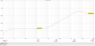
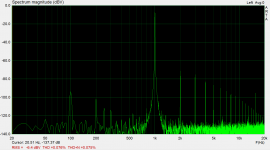
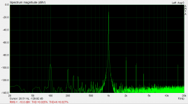
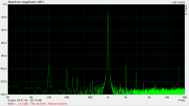
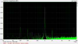
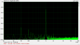
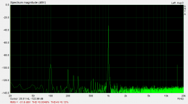
1.4A idle current, load 3R8 with output bjt, degeneration resistor bypassed :
18Vpp, 12Vpp, 8Vpp, 4Vpp, 2Vpp, 1Vpp
spike around 17KHz is a measurement / soundcard artifact..
18Vpp, 12Vpp, 8Vpp, 4Vpp, 2Vpp, 1Vpp
spike around 17KHz is a measurement / soundcard artifact..
Attachments
Last edited:
- Home
- Amplifiers
- Solid State
- Single Ended CFA