This amp was designed by Ian Hegglun, according to his
'Square Law' rules, as described in his articles:
IansArticles - Google Drive
and
AUDIO_EW-WW_Hegglun_Square-Law-Rules_Sep-1995_errata.pdf - Google Drive
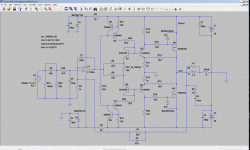
My attempt was to use hexfets as output devices.
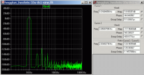
It sims very well, at least at 1kHz: 0.000381% THD (I guess due
to the use of the opamp at the input),
and seems to be relatively simple to build.
I think I'll try TL071 as an opamp.
Spice sim file + lib with models attached in zip file.
Will try to build 1-pair output, with rails at 35V,
60W output, which seems reasonable for a single pair.
Any input and suggestions are welcome.
Ian, anything changed since you published your articles?
It's been over 20 years..
'Square Law' rules, as described in his articles:
IansArticles - Google Drive
and
AUDIO_EW-WW_Hegglun_Square-Law-Rules_Sep-1995_errata.pdf - Google Drive
My attempt was to use hexfets as output devices.
It sims very well, at least at 1kHz: 0.000381% THD (I guess due
to the use of the opamp at the input),
and seems to be relatively simple to build.
I think I'll try TL071 as an opamp.
Spice sim file + lib with models attached in zip file.
Will try to build 1-pair output, with rails at 35V,
60W output, which seems reasonable for a single pair.
Any input and suggestions are welcome.
Ian, anything changed since you published your articles?
It's been over 20 years..
Attachments
Last edited:
Member
Joined 2009
Paid Member
all of Ian's ideas are worth trying
btw with used opamp it is peeky/resonant @ ~7.3MHz
but the performance @~1W is extraordinary
Pawel, do you have a model for TL071 ?
Hi minek123,...Any input and suggestions are welcome.
Ian, anything changed since you published your articles?
Thanks for starting this thread.
A lot did happen since that design was published - 3 more amp articles in Linear Audio - a simple square-law amp (vol1), the Cube amp (vol8) and the CSD amp (vol13).
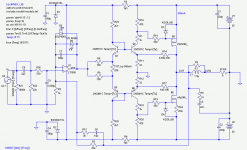
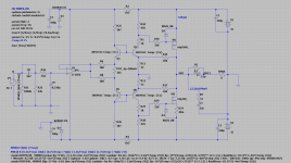
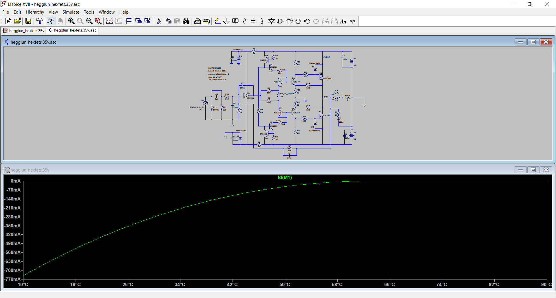
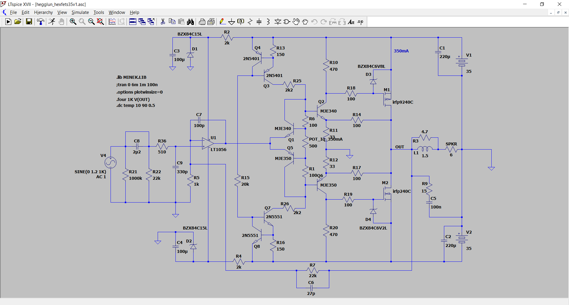
Attached is your circuit closer to original but with HEXFETs.
Local feedback R14,R17 they were around 10k in the original.
Added LED's across the opamp feedback to limit the swing for faster recovery from clip since the opamp only needs to output 0.5V to clipping the OPS.
R25,R26 to 15V directly.
Add R1,R23 series with drivers to limit dissipation when clipping. Lower power drivers can be used sine Pdis is now only 0.2W.
Increase gate R18,R19 for HF stability. Add R13 in series with shunt compensation C6 and trim C6 for optimum HF end.
Reduce R2,R4 for about 5mA through zeners with 35V rails.
Add source series resistor to p-channel to balance high current Gm. Trim R14 and Iq_POT for best linearity for 1W region.
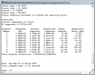
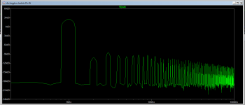
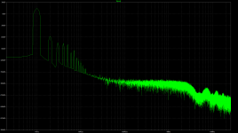
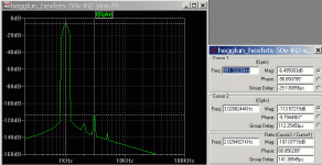
The FFT plot below for 1W at 1kHz
With HEXFET's some thermal linking with the bias is needed. I did try them without any linking and the amp blew up when I was demonstrating it to my electronics class
 . So I reverted back to laterals.
 The attached simulation shows about 25% linkage if both Q1 and Q5 are used as sensors, which is less than typical 70% thermal attenuation. Sensing could be done with only Q1 on the heatsink which would be closer to optimum.
Compensation of the original with R14,R17 around 10k is not easy; first gate resistors R18,R19 need to be large enough, much more than usual. Then C6 needs to be just right. Then R13 is added to C6 to minimise RF ingress back to the opamp.
For the original version C6 seems to be necessary for stability following clipping. It may be that if R14,R17 are reduced to say 100 ohms (like your version) then compensation may be easier. Maybe C6 could be eliminated with local feedback? I haven't tried this yet.
I have provided the original version as a base line.
Attachments
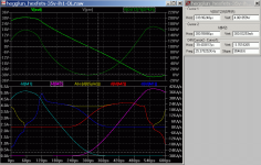
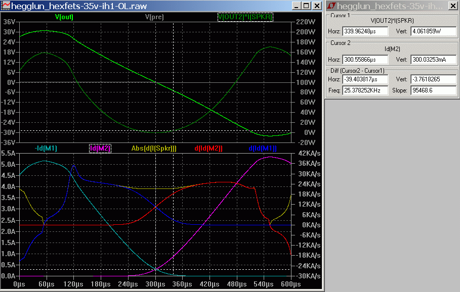
Here's the open loop plotsSuggestion: Do the sim without any global feedback (local around op-amp) then you get to see how well the square law works more clearly.
The linear flat region is with 300mA idle current and extends to nearly 1A or 4W peak (2W average). This is the square-law Class-A region.
Notice next to no local feedback is used here with R14,R17 around 10k. This is needed to see the native square-law region before extra feedback is applied using R14,R17.
BTW the OL circuit used to generate this plot is available in the previous post download zip.
Attachments
I came up with a slightly different topology along the same lines recently, not sure how it compares in performance: Is this a novel OS topology?
1) I previously tried to sim without CCS - feeding Q1/Q5 directly from zeners, like Ian suggested, but Thd went up..
I guess in real life it's simpler to go without CCS.
2) R14/R17 at 100 Ohm were chosen by Pavel Macura, who built something like this many years ago.
Not sure how he came up with value of 100
He used 2SJ118 + 2SK413 output devices (obsolete), which are not lateral, as far as I can tell.
3) Reasons I used MJEs for Q1/Q2/Q5/Q6 was that if we need thermal tracking, they need to be attached to the heatsink, and it's easier and more elegant with TO-126.
Besides, I have whole bucket of them...
Not sure how lowering their current affects Thd..
It's up 20 times (at full power); still very low though.
Also, since it sims very well with higher rails (say 50V instead of 35V), I guess it might be safer with MJEs...
Unless we can lower their current even further..
Interesting!Hi Minek, please look at this, much simpler topology,
it still has got gnfb but rather local, the graph looks great @~7W for such a simple circuit
The question is how to make it perform at higher wattage?
Say, at 70W (R14/R17 at 330 Ohm), THD is 1.5%
Pawel, do you have a model for TL071 ?
no, unfortunately not...
>I previously tried to sim without CCS - feeding Q1/Q5 directly from zeners, like
>Ian suggested, but Thd went up.
I repeated sims, and it doesn't actually make any difference. So no CCS needed.
Actually, I'm getting slightly better Thd when feeding Q1/Q5 directly from the rail
>Ian suggested, but Thd went up.
I repeated sims, and it doesn't actually make any difference. So no CCS needed.
Actually, I'm getting slightly better Thd when feeding Q1/Q5 directly from the rail
Nice and clean example of output stage with gain.
The absence of source resistors with devices having high transconductance/negative tempco makes me nervous, but it cannot be avoided if the square law principle is adhered to.
To mitigate the risks, I would overcompensate the thermal compensation.
In principle, for a "normal" compensation, coupling Q8/Q4 to the OPs would be sufficient, but for some reason, the amplifier is already hugely overcompensated:
I don't think it is possible (unless I missed something) in reality, it probably has to do with the models.
Anyway, I would redesign the base spreaders as Vbe multipliers, this allows overcompensation if required:
It is even more overcompensated, but it will probably be needed in reality
I wonder about the effect of R10/18/19/20 with the Miller capacitances of the MOS: I suspect they could limit the SR (I didn't simulate this aspect)
Attachments
Member
Joined 2009
Paid Member
Here's the open loop plots
The linear flat region is with 300mA idle current and extends to nearly 1A or 4W peak (2W average). This is the square-law Class-A region.
Notice next to no local feedback is used here with R14,R17 around 10k. This is needed to see the native square-law region before extra feedback is applied using R14,R17.
BTW the OL circuit used to generate this plot is available in the previous post download zip.
Impressive!
Does Nelson have something like this in one of his commercial amps? Uses a single pair of massive FETs without source resistors ?
Hi Bigun,Impressive! Does Nelson have something like this in one of his commercial amps? Uses a single pair of massive FETs without source resistors ?
Thanks. This HEXFET version seems more linear than the original lateral version. Probably due to the higher Gm per amp of these devices.
I think the F7 and F5 comes close in topology if you take off the opamp. They use jFET drivers so a simpler circuit. IIRC the F7 is essentially an F5 with laterals.
When I published my original circuit I thought my output stage alone gave low enough distortion with no high order harmonics. But I thought no one would be interested in it unless it had a lot of extra negative feedback and 0.001% distortion (or less) like Douglas Self's amps were moving toward. I did another version with a diamond input instead of the opamp for a reasonable input resistance.
Cheers,
Nice and clean example of output stage with gain.
The absence of source resistors with devices having high transconductance/negative tempco makes me nervous, but it cannot be avoided if the square law principle is adhered to.
To mitigate the risks, I would overcompensate the thermal compensation.
In principle, for a "normal" compensation, coupling Q8/Q4 to the OPs would be sufficient, but for some reason, the amplifier is already hugely overcompensated:
Elvee, Minek123,
Attached a 50V version with acceptable temp-comp using two Schottky diodes D9,10 on the heatsink. The thermal attenuation factor for zero-tc is 60% which I expect is on the heatsink near a power transistor. My sim can show this if the ".TEMP 25 75" card is enabled. But if the diodes are placed on top of the packages you should get overcompensation
 . One way to make mounting easier with say glass diodes is to glue them to a TO-202 (BD139) with a bolt. Note Q1,Q2 and Q5,Q6 are tied together and are not attached to the main heatsink.
For paralleling HEXFET's they need to be from the same batch and then matched for thresold voltage to within say +/-5mV. It is fairly easy to do with a 10k resistor in series with a 9V battery and measure the voltage from drain to source with the gate connected to the drain.
The attached sim now has the feedback resistors (R14,R17) 220 ohms and indeed I found the feedback capacitor across R7 can then be eliminated making it a lot easier to build. However, I found the distortion is higher with low values for R14,R17. I don't know why it is so.
Anyway, who needs such low distortion anyway
- with an output stage that has negligible high order harmonics even before global feedback is applied. But still, it may be useful for many designers to compare a 0.0003% amp to 0.003% just to prove for their own benefit if there is any benefit.Attachments
Hi Soundhappy,Interesting article The Square and Exponential Laws - Positive Feedback
Thanks for posting that. Good to see a transcript of Nelson's BAF 2019 talk on Square Laws and degeneration. BTW the printer friendly version allowed a PDF to be made and printed.
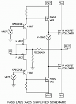
Nelson's XA-25 amp by Pass Labs is mentioned as not using source degeneration resistors in the jFET input stage or the MOSFET output stage. I found a review here Sneak Peek of the Pass Labs XA25 Class A Stereo Amplifier Review that is Coming Soon to Positive Feedback! - Jeff's Place and a thread here Pass XA25? and there are probably more. The topology of the XA-25 is given in the Positive Feedback article and (if allowed) below
It is basically an F5 with a cascoded input stage for a high rail voltage and a relatively low power "VAS" MOSFET stage driving BIG power MOSFET's as followers.
So the XA-25 is essentially the same topology as the square-law topology in this thread albiet beefed up for more volts and power. There are others who have used output stages with gain like here, and sorry if I have not mentioned them.
I was so pleased that Nelson told us how his friend Joe Sammut (RIP) could clearly distinguish between one of Nelson's undegenerated FET amps and the exact same but source degeneratated (see p4). he preferred the one without source degeneration. This is what convinced Nelson to develop his XA-25 without any source degeneration to get the best possible sounding amplifier.
My development of a square-law type amplifier back 25 years ago led me slowly to the realization that source degernation in MOSFET amplifiers is a backward step because it introduces higher order harmonics that need a lot of extra negative feedback to make them inaudible. Let's say we use 10dB of local source degeration in each side of a push-pull amp.
First, this lowers the optimum bias level, so you get less power in the 1W region where most of the action is.
Then you get more high order harmonics from "spectral growth distortion" (intermodulation from degeration itself) and to reduce high order harmonics we need to use maybe 2 times the amount of global feedback to reduce them back to the original low order harmonics with no degeration. This is because our hearing amplifes higher harmonics at the rate of up to 50dB per decade
. That means if we lose say 10dB from local degeration and need an extra 20dB (maybe 30dB?) to get back to original sound quality -- so we need 30dB just to break even (assuming 10dB of degeration). Then we still need some feedback to cover the distortion at the high power levels created by Class-AB MOSFET stages. That's the main reason we have to use huge amounts of negative feedback in our MOSFET power amplifiers.
If instead we don't use source degeration we can back off by 30dB of feedback (that's assuming 10dB of degeration). So the benefits of not using source degeration in MOSFET Class-AB amps are huge. The downside is a higher idle dissipation since without source degeration the bias level increases to get the low distortion levels in the target 1W region (that's assuming our speakers are reasonably efficient like 90dB/W/m or more). It doesn't require larger heatsinks than those rated for worst case dissipation. Just remember to turn your amp off when it is no longer required
.Attachments
Last edited:
- Status
- This old topic is closed. If you want to reopen this topic, contact a moderator using the "Report Post" button.
- Home
- Amplifiers
- Solid State
- Square Law Amp