I am not sure if this will catch interest but I am trying to design an amp with only one type of transistors, meaning either exclusively PNP or NPN. It should also have DC feedback meaning not the capacitor-coupled designs of the 70s.
Why? I guess for the fun. I didn't find a circuit around without transformers or coupling caps. Maybe its good to have on that day where they will stop making complementary bipolars
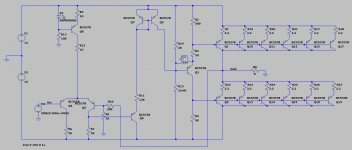
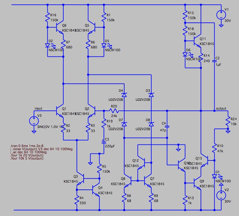
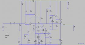
I have elaborated a first design with the BC557B which is a nice and cheap PNP transistor:
- Q6 is a current source for 2mA (R12 is the test resistor)
- Q4/Q5 are a differential pair for the feedback
until there, no problem.
- Normally after the differential, there is a complementary voltage amplifier. To avoid it, I put Q8 as emitter follower, and Q7/Q9 as current mirror. That way the voltage is transferred from the lower end to the upper end. The voltage on Q8 is converted to a current signal via R11.
- The output stage is from a 1962 book of a highly innovative transformer-free amplifier. I had a hard time researching for output stages without complementary transistors. After trying some designs, I understand why. A change in supply voltage requires recalculating the resistor values. Because the DC setpoints define these values, it can´t reach the full output voltage, in this case only ±7 of the ±15V. In addition some NTC must be added for thermal stabilization.
Some words on the design:
- Q6 current is 2mA (arbitrary)
- R6/R7 are 5K so the DC voltage along R7 is 5V with a swing of ±5V
- Q8 emitter voltage is that voltage plus 0.7
- The voltage on R11 is Q7 base voltage minus Q8 emitter voltage, or:
U11= (Vs -0.7) - (-Vs +5V +0.7V)
and the current swing is the voltage swing on R7 (±5V) divided by the value of R11. Here that means 2mA ±0,4mA. This sensitivity could be increased by placing a Zener diode in series with R11, because a voltage variation would then inherit a larger current variation.
- The current 2mA ±0,4mA is available on the collector of Q9. Q3 is a voltage amplifier. The design follows directly from the setpoints.
- Q3 base voltage is Vs - 2x 0.7 so 13.6V. The current through Q3 is chosen as 2.2mA.
- Q2 base voltage is the output voltage -0,7V.
- It is quite clear the design is not very clean, as Q1 is linked to the supply voltage while Q2 moves with the output voltage.
I would like to ask those people interested:
- At what point can this design be improved?
(This question is more on the general architecture, the stabilizing feedbacks and the thermal feedback can be added later).
- What options are available for the output stage?
(It seems the design is called totem-pole output and is used in tube amps and digital TTL circuits, but there are not too many information around concerning bipolar transistor amplifiers. Would a phase splitter with two independent voltage amplifiers bring any improvement?)
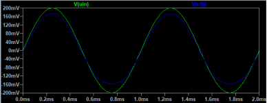
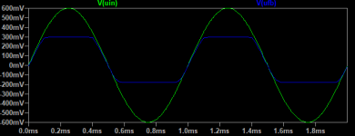
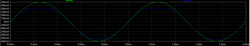
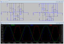
I have added the Spice schematic as asc and screenshot, and two simulation results. It works in principle, but not very well.
Thanks
Why?
I guess for the fun. I didn't find a circuit around without transformers or coupling caps. Maybe its good to have on that day where they will stop making complementary bipolars I have elaborated a first design with the BC557B which is a nice and cheap PNP transistor:
- Q6 is a current source for 2mA (R12 is the test resistor)
- Q4/Q5 are a differential pair for the feedback
until there, no problem.
- Normally after the differential, there is a complementary voltage amplifier. To avoid it, I put Q8 as emitter follower, and Q7/Q9 as current mirror. That way the voltage is transferred from the lower end to the upper end. The voltage on Q8 is converted to a current signal via R11.
- The output stage is from a 1962 book of a highly innovative transformer-free amplifier. I had a hard time researching for output stages without complementary transistors. After trying some designs, I understand why. A change in supply voltage requires recalculating the resistor values. Because the DC setpoints define these values, it can´t reach the full output voltage, in this case only ±7 of the ±15V. In addition some NTC must be added for thermal stabilization.
Some words on the design:
- Q6 current is 2mA (arbitrary)
- R6/R7 are 5K so the DC voltage along R7 is 5V with a swing of ±5V
- Q8 emitter voltage is that voltage plus 0.7
- The voltage on R11 is Q7 base voltage minus Q8 emitter voltage, or:
U11= (Vs -0.7) - (-Vs +5V +0.7V)
and the current swing is the voltage swing on R7 (±5V) divided by the value of R11. Here that means 2mA ±0,4mA. This sensitivity could be increased by placing a Zener diode in series with R11, because a voltage variation would then inherit a larger current variation.
- The current 2mA ±0,4mA is available on the collector of Q9. Q3 is a voltage amplifier. The design follows directly from the setpoints.
- Q3 base voltage is Vs - 2x 0.7 so 13.6V. The current through Q3 is chosen as 2.2mA.
- Q2 base voltage is the output voltage -0,7V.
- It is quite clear the design is not very clean, as Q1 is linked to the supply voltage while Q2 moves with the output voltage.
I would like to ask those people interested:
- At what point can this design be improved?
(This question is more on the general architecture, the stabilizing feedbacks and the thermal feedback can be added later).
- What options are available for the output stage?
(It seems the design is called totem-pole output and is used in tube amps and digital TTL circuits, but there are not too many information around concerning bipolar transistor amplifiers. Would a phase splitter with two independent voltage amplifiers bring any improvement?)
I have added the Spice schematic as asc and screenshot, and two simulation results. It works in principle, but not very well.
Thanks
Attachments
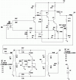
the Sony TA1010
Thank you. This shows that it can work perfectly. The output stage is very well done, especially the various correction circuitry that it has. I haven't seen such a good "single type" design yet.
Thanks, yes you did and I found it: 117260-challenge.html.I threw this challenge to the forum
But - There are only 2 schematics.
The first has a very nice input stage with also emitter followers and current mirrors in it - it is the same as my (very basic) suggestion, however, the system is made twice for each output of the differential amplifier, and the two current mirrors are then coupled to achieve balance. The DC gain is improved by substracting the output current from a current source (I had 1.6-2.4mA and with this system it becomes 0 - 0.4mA for the push and the pull stage) which is again a very smart idea to compensate for the workaround with the emitter follower/current mirror. The caps C1 C2 are optional but if they would be used I guess they could damage the transistors Q12 Q13 at powerup.
The problem remains the connection to the output stage - a constant-current class A is nothing I want. Why hasn't it been completed?
The other proposal has 3 power supplies (although the third could be realized with some series diodes) but this design is more a concept and leaves too many questions.
It's the same design if the power supply and diodes are reversed. I'll go with NPN for this thread.Why not NPN types instead

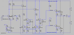
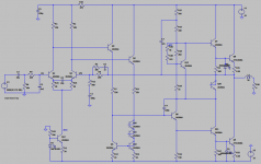
I try to go forward with the output stage of the TA1010 (push-pull), and the input stage/VAS design of the "npn challenge". However I don't manage to hook both together. The attached circuit somehow works but the resistances must be perfectly balanced, and the bias current is totally out of control.
I have two current mirrors drawing from 0-0.4mA each time for the push and the pull, respectively. Meaning "pulling current" on Q15 (or Q17) should "increase current" of the respective output leg Q6/Q5 (or Q9/Q8).

I've been thinking about many variants but couldn't imagine one without complementary transistors. So for this design, npn only. If you have an idea please let me know, thanks.
Attachments
> exclusively PNP or NPN. It should also have DC feedback meaning not the capacitor-coupled designs of the 70s.
This is essentially equivalent to a tube amp (all tubes are N-type). The problem is that each device's output (plate, collector) winds up more positive than its input (grid, base). So node voltages stack-up until they hit the ceiling.
Yes, there are tricks. The 2-bottle op-amp runs a couple neon lamps between stages to drop 180V. Mark's #7 plan is the same in sand.
Also a BJT "can" have collector lower than base, by a half-volt which isn't much. LM324 uses that fact but is liberal with P-types. (And its output stage sucks; it is for automotive instrumentation not fine audio.)
If you like class A, the original JLH amp is all N-type output stage and full push-pull, but the drive is near the negative rail and makes DC-centering input stage awkward.
You did not prohibit transformers. There are many topologies which fit your strange constraint. Obviously a tube-type CT output transformer. But there was a class of totem-pole with base transformer but direct coupled to a speaker. Frequently the "DC centering" was casual, semi-matched or trimmed bias resistors and 1V DC offset on the speaker. Literally good enough for Jazz (Fender Rhodes).
I am not sure if this will catch interest but I am trying to design an amp with only one type of transistors, meaning either exclusively PNP or NPN. It should also have DC feedback meaning not the capacitor-coupled designs of the 70s.
Looks good.
What do you intend to do? is it just that you know if its possible? then here my answer. Yes it is.. No problems.
But why so many BC557? what are you going to drive? What's the load?
My Idea of a good Amp is as little parts as possible.. especially with Transistors..
You will need to cut the Grades that all of them Working similar otherwise you will get unwanted distortion of any Kind.
Keep it simple.. it's not a question of NPN or PNP and it's not a question of Complimentary or Quasi complimentary.
One more thing is DC Feedback, try to use as little as possible. I think using a PID or a DC comparator to remove unwanted DC Output at output.Using DC comparator has the advantage of not actively injecting into "Signal Path" as a negative Feedback does.
Hope this helps you in one or the other way.. Just some thoughts on this matter.
NPN only
Well it seems you have to be quick or your post get trashed.
Some of these circuits have the "DHL" problems. I'd explain those but this has to be short. A partial solution is to use a diode. Here are a couple such circuits.
But I have a new idea to use a current mirror. This version lacks some refinements like feed forward cap and thermal compensation but you should get the idea. Have fun with it.
Attachments
You did not prohibit transformers. There are many topologies which fit your strange constraint. Obviously a tube-type CT output transformer. But there was a class of totem-pole with base transformer but direct coupled to a speaker. Frequently the "DC centering" was casual, semi-matched or trimmed bias resistors and 1V DC offset on the speaker. Literally good enough for Jazz (Fender Rhodes).
I didn't even think of a transformer based class B output stage when considering this part of the amp (I gave up!), but its the obvious approach as used extensively in early transistor circuitry.
Nice workaround to replace a pnp current source. I picked it up.The output stage is more daunting
In the linked "challenge" thread, it was said this design job would be trivial. Still I haven't seen a schematic that can compete with a normal complementary amplifier. (At least, before getting steveu's solution on page 1)This is essentially equivalent to a tube amp
Absolutely - pnp and npn are normally alternating and this has established itself so much. But there are tricks.The problem is that each device's output (plate, collector) winds up more positive than its input (grid, base).
I plan to use it in my everyday life, so quiescent current should be minimal, therefore I would only build a push-pull stage. In a book it was said a push-pull could be a Class A as well but anyway I want push-pull.If you like class A
Yes there are plenty of transformer-based designs around which I would consider. You can properly design your DC coupling and bias control with it.You did not prohibit transformers
I am looking for a build because I need another Amp in my hoome. I have build something more common before, I am happy with it and it was fun, I use that Amp, but now I look for a design challenge and something new.What do you intend to do? is it just that you know if its possible? then here my answer. Yes it is.. No problems.
I disagree with the no problem. I have put my mind on this already several times, even years back, and I never got to something I would build, that's the reason for the thread.
I agree that I got totally lost with my last schematic. I would use one type of Transistor (not sure if for the output a power npn or rather 10-20 TO92s in parallel), some resistors, Diodes, and caps.as little parts as possible
Complimentary transistors will be accepted, complementaries not.complimentary
[Sorry I had to place this one]
That would be the TA1010 in the first reply. I am surprised by its performance, at least in the simulation. However - I guess this is not so easy to realize.DC Feedback, try to use as little as possible
D1 is the key. You made it. Wow.Here are a couple such circuits.[...]Have fun with it.
Questions:
- What does DHL stand for? Are there literature references?
- Is your proposal something common or new? Any relations to the totem-pole where they also put a diode?
- What is the idea of C2 as it works without?
- 180mA bias? On purpose or just a first design?
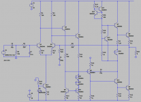
- I added a current source Q13, and emitter resistors in the input. The result is more or less the same in sensitivity but Q1 and Q2 must not match so well.
- I added 2 diodes on the collector of Q10. In R7 and R11 the voltage is actually converted to a current signal, with the diodes some balance is achieved.
- I removed the C2 and replaced the resistors initially by an 8ma current source. The win is parameter independence towards supply voltage. I have later found out that your resistor proposal is better for balancing. Finally I put a current source with 2.1k for the bias. Compared to a sole 2.1k resistor, it improves the symmetry of operation, the reasons are a bit unclear yet.
- I would extended the "bias generator" Q12/R18/R19, if you want to call it that way, with an NTC (5k at 24°C and 2.5k at 50-60°C) for temperature stabilization.
The result is quite similar to the Amp designs we all know from the textbooks.
But - with only npn Transistors. For the additional cost of: few diodes, two emitter followers and one current mirror.
You can't believe how many thoughts I gave this mistery and you just post something... It looks so simple...
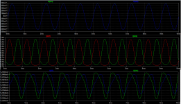
I will continue to work on the circuit, but as it looks now this could become a build.
For the idea with the mirrors, let me know if there is progress.
Attachments
It's important that R17 be smaller than, in this case, R26 so that under no circumstances can the vas current turn on Q9 without current from the diode (Q18).
Sorry, it's not "DHL" but "JLH" or "DLH", a dreadful old design with massive shoot-through current and distortion when driving reactive loads. I wrote an explanation but took too long and that post got lost to the timeout.
Sorry, it's not "DHL" but "JLH" or "DLH", a dreadful old design with massive shoot-through current and distortion when driving reactive loads. I wrote an explanation but took too long and that post got lost to the timeout.
The LTP current source may improve THD a bit but not much. Like wise the vas current source but the advantage of a bootstrap is that it adds a couple volts swing to the output rather than wasting a bit in the current source. You can bootstrap a current source.
Ya, the bias is too high, but this version has a bit too much THD otherwise. You can push the OLG by partial bypass RC networks across R7 and R11. I used 1uf and 10K each.
Ya, the bias is too high, but this version has a bit too much THD otherwise. You can push the OLG by partial bypass RC networks across R7 and R11. I used 1uf and 10K each.
It is evoluting.
Hi steveu,
Thanks for your your update.
The filter to provide constant supply R23 and C5, is a good proposal.
Q5/Q10 is not a current mirror anymore - Q4 is not forwarding its work to the output stage. I believe it should be a modified EFA circuit, or a combination with a voltage source (which is more smart than my dumb two diodes), but current mirroring doesn't seem to work well when there is R28. As it is important that R7 and R11 have the same voltage (at input 0) I will keep the 2 diodes before Q10. The voltage source would be 2 resistors and 1 transistor, versus just 2 diodes or transistors.
The 2N3055 are one big reason for not achieving too much similarity on the push and pull stage, and the wild bias current. It's a banana. I assume there's a reason why single-type amps had always been built with a transformer or Cap, back in the days when complementary transistors were expensive and avoided. So a good transistor is a must.
You had mentioned R17 < R4 to avoid issues at inductive loads - I can't follow this reasoning. The complete base current of Q9 comes from D1, even if I put heavy inductive loads. I put R17=R4 to have the same quiescent conditions. I reduced R16 from 1k to 720 Ohm to achieve same AC conditions.
You are correct for the "current source" I had put instead of R10 - it can just be a bootstrap. The output stage is a class A (with Q6) push-pull. I have also left a Cap, however I reduced it from 220u to 47n in order to avoid an electrolytic. The small cap is helping in stability and supports disturbance suppression - I don't see the need for a large value as large, slow swings can be handled well with the feedback.
What else did I play with?
For stability, as mentioned I keep the cap in the bootstrap of the driver but much smaller. I keep the cap of the amplifier Q6. I added a cap in the differential amp. I added a cap in the feedback voltage divider. Both last ones prevent oscillations if you hit saturation. Looks good now.
The current mirror on the input stage is good concerning independence to supply voltage. I understand it doesn't affect THD too much, but the results are still a bit better.
For the amplifier stage (Q6) I connect its collector to the Q12 emitter instead of the GND. It doesn't affect operation too much, but the output drivers Q7 and Q11 will have identical quiescent conditions. I also see an improvement in the crossover point, it is more smooth and the transistors don't turn on/off that fast. Without it I think the push and pull stage will always have different conditions.
I modified the feedback resistors with the cap bypass for stability.
Added LEDs in parallel to the power transistors for current limiting. A 1,65V red LED and a 0.26 Ohms emitter resistor will limit to 3.5A. That's basic stuff.
Thermal control. I add an NTC 5k (5k at 25°C, more or less 2.5k at 50°C) in parallel to the voltage generator R18. The bias current will be reduced at increasing temperature. It's old-fashioned but cheap and very reliable. So this gives me 6mA and 180mA at 25°C, and 1mA and 5mA at 50°C. I know the Hifi will become Lowfi but to me reaching 50°C just means the heatsink is too small.
For more gain a second stage of the differential amplifier could be added. But more gain means again stability needs review.
I feel quite confident with this design. Performance and stability are good. I think there is potential in your mirror proposal. I'll wait for more feedback and I'm looking forward for the build.
I will use BC567 and TIP35c in the test. I think about using only the type 2SC2655 later, so 7 in parallel for the output, I never worked with Japan transistors before and this seems to be an universal champ with constant hFE from 10mA to 0.5A - this will highlight the "single type" design.
Hi steveu,
Thanks for your your update.
The filter to provide constant supply R23 and C5, is a good proposal.
Q5/Q10 is not a current mirror anymore - Q4 is not forwarding its work to the output stage. I believe it should be a modified EFA circuit, or a combination with a voltage source (which is more smart than my dumb two diodes), but current mirroring doesn't seem to work well when there is R28. As it is important that R7 and R11 have the same voltage (at input 0) I will keep the 2 diodes before Q10. The voltage source would be 2 resistors and 1 transistor, versus just 2 diodes or transistors.
The 2N3055 are one big reason for not achieving too much similarity on the push and pull stage, and the wild bias current. It's a banana. I assume there's a reason why single-type amps had always been built with a transformer or Cap, back in the days when complementary transistors were expensive and avoided. So a good transistor is a must.
You had mentioned R17 < R4 to avoid issues at inductive loads - I can't follow this reasoning. The complete base current of Q9 comes from D1, even if I put heavy inductive loads. I put R17=R4 to have the same quiescent conditions. I reduced R16 from 1k to 720 Ohm to achieve same AC conditions.
You are correct for the "current source" I had put instead of R10 - it can just be a bootstrap. The output stage is a class A (with Q6) push-pull. I have also left a Cap, however I reduced it from 220u to 47n in order to avoid an electrolytic. The small cap is helping in stability and supports disturbance suppression - I don't see the need for a large value as large, slow swings can be handled well with the feedback.
What else did I play with?
For stability, as mentioned I keep the cap in the bootstrap of the driver but much smaller. I keep the cap of the amplifier Q6. I added a cap in the differential amp. I added a cap in the feedback voltage divider. Both last ones prevent oscillations if you hit saturation. Looks good now.
The current mirror on the input stage is good concerning independence to supply voltage. I understand it doesn't affect THD too much, but the results are still a bit better.
For the amplifier stage (Q6) I connect its collector to the Q12 emitter instead of the GND. It doesn't affect operation too much, but the output drivers Q7 and Q11 will have identical quiescent conditions. I also see an improvement in the crossover point, it is more smooth and the transistors don't turn on/off that fast. Without it I think the push and pull stage will always have different conditions.
I modified the feedback resistors with the cap bypass for stability.
Added LEDs in parallel to the power transistors for current limiting. A 1,65V red LED and a 0.26 Ohms emitter resistor will limit to 3.5A. That's basic stuff.
Thermal control. I add an NTC 5k (5k at 25°C, more or less 2.5k at 50°C) in parallel to the voltage generator R18. The bias current will be reduced at increasing temperature. It's old-fashioned but cheap and very reliable. So this gives me 6mA and 180mA at 25°C, and 1mA and 5mA at 50°C. I know the Hifi will become Lowfi but to me reaching 50°C just means the heatsink is too small.
For more gain a second stage of the differential amplifier could be added. But more gain means again stability needs review.
I feel quite confident with this design. Performance and stability are good. I think there is potential in your mirror proposal. I'll wait for more feedback and I'm looking forward for the build
. I will use BC567 and TIP35c in the test. I think about using only the type 2SC2655 later, so 7 in parallel for the output, I never worked with Japan transistors before and this seems to be an universal champ with constant hFE from 10mA to 0.5A - this will highlight the "single type" design.
Attachments
- Home
- Amplifiers
- Solid State
- Amplifier with only 1 type of transistors