Using a VBE multiplier instead of R45 would improve the thermal stability.
The only way to kill the current mirror must be because the driver dies , but Q18 current limit should prevent that. There should never be more than ~3VDC on the current mirror transistors, ie 100mW Be sure your 2K resistors are not maybe 200 Ohms.
The only way to kill the current mirror must be because the driver dies , but Q18 current limit should prevent that. There should never be more than ~3VDC on the current mirror transistors, ie 100mW Be sure your 2K resistors are not maybe 200 Ohms.
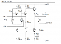
uA702
I'm tempted to spend the time to simulate a uA702 to find out just how bad it was but I can see from the schematic that the output is single ended class-A and hi-Z (2.6K+) on the negative side, but most important is that the output voltage is limited to something less than 50% of the supply voltage shifted down in order to cover zero, ie become somewhat bipolar. uA702 was never popular for good reasons. If you are bored, do a simulation and I expect you will get a maximum of 9V P-P unloaded and maybe 6Vp-p into 1K using a 21VDC supply. This was useful for small signals and it was fairly fast, but useless as a power amplifier design.
μA702
Correct... I should have said, npn-only class AB, without the coupling caps or transformers.
I'm tempted to spend the time to simulate a uA702 to find out just how bad it was but I can see from the schematic that the output is single ended class-A and hi-Z (2.6K+) on the negative side, but most important is that the output voltage is limited to something less than 50% of the supply voltage shifted down in order to cover zero, ie become somewhat bipolar. uA702 was never popular for good reasons. If you are bored, do a simulation and I expect you will get a maximum of 9V P-P unloaded and maybe 6Vp-p into 1K using a 21VDC supply. This was useful for small signals and it was fairly fast, but useless as a power amplifier design.
Incidental: vintage words from Bob Widlar...
https://www.edn.com/future-trends-in-ic-operational-amplifiers/
https://www.edn.com/future-trends-in-ic-operational-amplifiers/
I haven't managed to get the first build stable. I did discover several mistakes in the PCB, especially diode positions etc.
I have simplified the schematic and removed all I could, the VAS is only 1 transistor, current mirror only 2 transistor, and I used simple resistors when possible. The goal is to get this stable first. However there is a remaining oscillation around 600kHz. By adjusting the VAS it appears as the positive side is stable but once a signal gets negative the oscillation starts.
My plan is to do a new PCB with the simplified schematic (I had used the complicated circuit PCB in the second try) and I add space for stabilizing elements (capacitors, base resistors), but I also add a PNP transistor as a driver for the bottom power transistor (although I'm convinced that the bottom driver is the cause).
Any thoughts where the problem is from are welcome.
Oh one main thing has changed. I did add a Vbe multiplier in line with the resistor at the input side of the current source. This seems perfect for thermal compensation, but it also simplifies the whole mechanism. I have written down all the equations of this circuit - in the theory this amp is perfectly symmetric and linear, especially the relationship between the VAS voltage and the speaker voltage.
Attachments
I should explain. This PNP transistor is an option to build a conventional quasisymmetric output first, get a amp stable, and then remove the PNP and go on from there to the new npn-only output stage.but I also add a PNP transistor as a driver for the bottom power transistor
Some possibilities.
1. Start by removing C2 (47p). If that stabilizes the oscillations then try adding a series ~10k resistor to C2 then smaller and smaller until it oscillates again and then back off.
2. Add a Zobel network to the output.
3. If all else fails increase C7.
1. Start by removing C2 (47p). If that stabilizes the oscillations then try adding a series ~10k resistor to C2 then smaller and smaller until it oscillates again and then back off.
2. Add a Zobel network to the output.
3. If all else fails increase C7.
Results from a new PCB with the simplified circuit
I have now redone a new PCB with the simplified version with some added base resistors. I had previously build the same simplified circuit on the initial PCB and failed. But now with a more clean board, the issues are less critical.
The main issue (oscillation on lower half cycles, see post 46) was solved with a base resistor on the current mirror R16. This is even visible in the simulation at f=1k (sine) and R16<20 and C2=0. It disappears on R16=47 and on my PCB at R16=20. (oftentimes base resistors are used to stabilize current sources)
When reducing C7 from an initial 220p where everything was nice down to 100p, another oscillation comes up at rectangular signal. This is visible in the simulation at f=20k (square) and C2=0. Indeed if C2 is added at 100p this also disappears.
A difference between reality and simulation is that I need a Vbe multiplier with 3*0.65V Q6/R3/R9 plus a diode D8 1N4148. In the simulation that voltage drop is much less. The thermal compensation is overcompensating with 3*Vbe.
Hum is an issue as 100u are not enough after R23. The input stage consumes 5,5mA.
Without C2 every internal signal is harmonic and by adding C2=100p things get a bit spiky. I assume this is the stabilizing action. I will evaluate your proposal to add a resistor in line with C2, but the simulation reacts a bit differently than the real thing. Also I need to add Zobel and see how a speaker reacts, the tests were done with a resistor.
Attachments
Some interesting problems with simulating a square wave.
1. If you set/leave the rise and fall time at zero, you get about 5uS for both. If you set them to 1p then you get a much faster rise and fall time. Probably a default "feature".
2. The "initial" voltage for the pulse is used in the initial condition calculation for the coupling caps and creates an offset for the time constant for (C3) the input coupling cap. I found no way to get rid of this offset except running the simulation long enough for it to settle and set the simulation start of data afterwards. Reducing C3 helps. You can short out the coupling caps C3 and C1 but ... This is not a problem for a sine because the initial and negative peaks values are not the same thing.
3. 10KHz square waves and 10K bias resistors are not a good mix because you need current to drive capacitance quickly. Also, you need the resistors from the current mirror to ground in order to get most of the supply swing output. This also applies to the VAS pull-up R30.
4. Similarly, the 100 Ohm base resistors are slow to turn off the power transistors. A diode across the EB of Q13 allows the VAS to pull current out of Q8 and turn it off much faster. On the lower side, adding another transistor to the current mirror for a second output can drain Q9 faster than a 100 Ohm resistor, provided the bias resistors are ~1K and not 10K.
5. Mirror degeneration resistors have to be kept as small as possible because they are extra voltage drop that may cause a minimum current in Q9, ie never turns off.
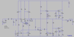
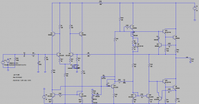
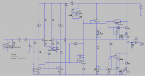
The attached schematic illustrates these ideas although I'm sure there is more work to be done.
1. If you set/leave the rise and fall time at zero, you get about 5uS for both. If you set them to 1p then you get a much faster rise and fall time. Probably a default "feature".
2. The "initial" voltage for the pulse is used in the initial condition calculation for the coupling caps and creates an offset for the time constant for (C3) the input coupling cap. I found no way to get rid of this offset except running the simulation long enough for it to settle and set the simulation start of data afterwards. Reducing C3 helps. You can short out the coupling caps C3 and C1 but ... This is not a problem for a sine because the initial and negative peaks values are not the same thing.
3. 10KHz square waves and 10K bias resistors are not a good mix because you need current to drive capacitance quickly. Also, you need the resistors from the current mirror to ground in order to get most of the supply swing output. This also applies to the VAS pull-up R30.
4. Similarly, the 100 Ohm base resistors are slow to turn off the power transistors. A diode across the EB of Q13 allows the VAS to pull current out of Q8 and turn it off much faster. On the lower side, adding another transistor to the current mirror for a second output can drain Q9 faster than a 100 Ohm resistor, provided the bias resistors are ~1K and not 10K.
5. Mirror degeneration resistors have to be kept as small as possible because they are extra voltage drop that may cause a minimum current in Q9, ie never turns off.
The attached schematic illustrates these ideas although I'm sure there is more work to be done.
Attachments
old patents
I couldn't believe this received a patent until I looked at the date, 1958. This circuit is related to the diode circuit but with more problems. And the IPS uses a transistor of the opposite polarity. Most of the transistors are PNP because most Germanium transistors were PNP and that's what they had in 1958.
I couldn't believe this received a patent until I looked at the date, 1958. This circuit is related to the diode circuit but with more problems. And the IPS uses a transistor of the opposite polarity. Most of the transistors are PNP because most Germanium transistors were PNP and that's what they had in 1958.
Yes if R10 and R25 are replaced by 1k it is much better, but that consumes a lot of quiescent current. And the VAS also needs to be supplied via a smoothed voltage to prevent hum, ok it is only a basic VAS with the 10k resistor. Replacing the 100 Ohms of Q26 by an other transistor or other value doesn't change much if the resistors are not also changed to 1k. But it is an important behavior to understand the bottleneck.
I would believe that foremost the turn-on and turn-off of Q9 is too slow:
- Works (much) better with R25 1k than 10k
- the problem is mostly from the lower part
- it helps to add a voltage source and diodes to the output stage (similar to the VAS clamp) to ensure the transistors are never fully turned off, but keep some mA.
- The feedback will rather let Q9 do what it does (be slow) and control Q8 to correct the difference (fast, so that the difference of both currents is the output). So going "down" is an issue as Q8 is turned off fast but Q9 not on yet. Going "up" is an issue as Q8 fives extracurrent as Q9 still turns off. Quite unlucky, as one of the few benefits of using same transistors could be to have identical behavior.
Maybe the current source cannot drain the lower driver?
It is interesting to see the effect of resistors in line with the 100pF cap C7. It may be the "one" solution concerning stability, to suppress the oscillations arising on the lower half wave, the current mirror base resistor can be avoided thereby.
I have replaced C7 by two parallel RCs
--R10k--100pF--
--R2k7--100pF--
(It is also possible to keep C7 and put a RC with 3k 100pF in parallel, and it is also ok to use 1k and 2k7).
The use of C2 (47pF from VAS collector to current mirror) is then also without negative effects.
@steveu, could you please explain the original idea behind C2?
Higher C2 means faster "up" and slower "down" in the simulation, so it could be nice for balancing speed, but in reality I see no effect (tried 0 22 47 and 100pF, no big difference).
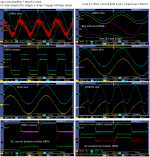
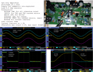
-> Below results with EB diode on Q13 and C2=47pF and modified C7.
-> I noticed too late that only 10V supply, and the current limit is also a bit strict.
-> I would say this is not too bad, but can be improved
Just a thought. A feature of the current mirror topology is that R30 (VAS pullup) and R10 (input to current mirror) have the identical AC current, but opposite sign. It means, the VAS driver signals are actually made available in opposide signs - like with a phase splitter. While a phase splitter would deliver only voltage, the lower part of the current mirror delivers the VAS signal as current, which is what is needed for npn-only:
* upper EF output stage operates in voltage mode, fed by VAS voltage,
* lower EF output stage operates in current mode, fed by VAS current.
Thereby maybe the R25 should be questioned - we have the VAS current as current, for an EF in current mode, but we use a voltage signal to drive.
I would believe that foremost the turn-on and turn-off of Q9 is too slow:
- Works (much) better with R25 1k than 10k
- the problem is mostly from the lower part
- it helps to add a voltage source and diodes to the output stage (similar to the VAS clamp) to ensure the transistors are never fully turned off, but keep some mA.
- The feedback will rather let Q9 do what it does (be slow) and control Q8 to correct the difference (fast, so that the difference of both currents is the output). So going "down" is an issue as Q8 is turned off fast but Q9 not on yet. Going "up" is an issue as Q8 fives extracurrent as Q9 still turns off. Quite unlucky, as one of the few benefits of using same transistors could be to have identical behavior.
Maybe the current source cannot drain the lower driver?
It is interesting to see the effect of resistors in line with the 100pF cap C7. It may be the "one" solution concerning stability, to suppress the oscillations arising on the lower half wave, the current mirror base resistor can be avoided thereby.
I have replaced C7 by two parallel RCs
--R10k--100pF--
--R2k7--100pF--
(It is also possible to keep C7 and put a RC with 3k 100pF in parallel, and it is also ok to use 1k and 2k7).
The use of C2 (47pF from VAS collector to current mirror) is then also without negative effects.
@steveu, could you please explain the original idea behind C2?
Higher C2 means faster "up" and slower "down" in the simulation, so it could be nice for balancing speed, but in reality I see no effect (tried 0 22 47 and 100pF, no big difference).
-> Below results with EB diode on Q13 and C2=47pF and modified C7.
-> I noticed too late that only 10V supply, and the current limit is also a bit strict.
-> I would say this is not too bad, but can be improved
Just a thought. A feature of the current mirror topology is that R30 (VAS pullup) and R10 (input to current mirror) have the identical AC current, but opposite sign. It means, the VAS driver signals are actually made available in opposide signs - like with a phase splitter. While a phase splitter would deliver only voltage, the lower part of the current mirror delivers the VAS signal as current, which is what is needed for npn-only:
* upper EF output stage operates in voltage mode, fed by VAS voltage,
* lower EF output stage operates in current mode, fed by VAS current.
Thereby maybe the R25 should be questioned - we have the VAS current as current, for an EF in current mode, but we use a voltage signal to drive.
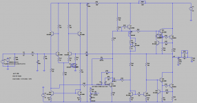
Attachments
Last edited:
Actually the base current of the lower driver is a severe disturbance to the current mirror. For example: a load of 4 Ohm, output -8V, we have 2A. But in the 10k resistor we have around 1mA as the output is lowered, and as this mA all goes to the driver, the current source is already at 0mA. In practice actually the amp newer could draw more than 2A.
Adding pre-drivers for a three-stage EF output is a solution. With 22V it can reach around 17V output swing on positive and negative rails. Not sure is base stopper resistors will be needed.
Also added a CCS to eliminate hum. Thermal compensation should normally not be needed with the current mirror as the Vbe drop is same in the upper and lower part, however in the build the bias falls as temperature increases, so R9 will be a resistor network with a NTC, values to be determined later.
Attachments
Almost a year gone since the last post. The npn-only-Amplifier is now working quite well.
The last prototype is partially built with SMD transistors as you get them as dual package, but that made more trouble than the circuit design. TSSOP-6: never again.
Stability is excellent. There is a 100pF Miller capacitor in parallel to a R=2k7 and 47pF. All base stopper resistors including the ones in the current mirror have been removed.
Operation is quite symmetric with no noteable crossover effect as long as there's enough idle current. The transistor choice is really basic, effects start to be visible at 20kHz with idle currents smaller than 10-20mA.
What's not so good:
I'll now review this thread and scan for all the tips and think about them again. And build the next one in TO-92.
The last prototype is partially built with SMD transistors as you get them as dual package, but that made more trouble than the circuit design. TSSOP-6: never again.
Stability is excellent. There is a 100pF Miller capacitor in parallel to a R=2k7 and 47pF. All base stopper resistors including the ones in the current mirror have been removed.
Operation is quite symmetric with no noteable crossover effect as long as there's enough idle current. The transistor choice is really basic, effects start to be visible at 20kHz with idle currents smaller than 10-20mA.
What's not so good:
- Quite a temperature dependency of the idle current, but not too bad. I believe an NTC parallel to R9 to limit startup current will be sufficient.
- The current limiter works terribly on the lower side and creates heavy oscillations when active (while the top one is very fine). In the simulation that was working but in the prototype it is not.
I'll now review this thread and scan for all the tips and think about them again. And build the next one in TO-92.
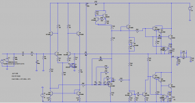
Attachments
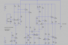
I was thinking about this and wondering if I could improve on the idea. I wasn't sure it would help but the simulation seems to work well. The idea is to use a NPN transistor backwards to compare the VAS voltage to the output, perhaps a bit more accurate than just a current mirror. The result also deals with the negative saturation limit and a degen resistor allows you to adjust the local loop gain for stability. You can use a CCS for the VAS pull-up but I prefer a bootstrap. LV's improved two wire CCS might have a use here.
Attachments
The problem with the current mirror and resistors as a diff-amp is that inaccuracies in the current mirror translate to a significant offset, which means unpredictable idle current in this situation. But the Vbe voltage threshold of Q15 is well defined. I don't think you are going to get a symmetric XO without complementary devices, and maybe that's not a bad thing. Note that the simulation saz this version manages a THD less than 0.01%. We know that 2nd order distortion can be very appealing. Some people are building quasi amps because they want 2nd order harmonics. The idea of a NPN only circuit is a novelty and not a means to the best performance. It might be useful for monolithic circuits, but manufacturers seem to have managed PNP devices on chip that work well enough.
In tube amps the even harmonics appear gradually whereas in this case they will appear with a discontinuity at the crossover point (IE crossover distortion without the odd harmonics). I am hesitant to accept this is a very desirable way to introduce 2nd harmonics. I won't die on that hill though.
What happens if you feed R1 from the bootstrap? It is effectively shunting the VAS node. If sharing a bootstrap worsens the bias stability it might benefit from it's own bootstrap. Nevermind, it would have to be bootstrapped from Q16's emitter, which is counterproductive.
The current mirror is comparing the currents in R11 and R12, a poor form of diff-amp. R1 and R12 need to terminate at the same point because Q15 is near off until you need negative output current and the current in R11 drives the lower output off (Q12,13). The actual voltage on the collector of Q15 is a bit below the positive rail, at a point where the idle current is found, and where the currents in R11 and R12 are almost the same. The closer the value of R12 is to R11, the closer to the rail the collector of Q15, but it has to be something lower than the rail so R11 has to be less than R12. Unlike the earlier circuit, R12 is fed from the rail so there is always current available to drive the output to the negative rail. Perhaps there is a hazard to the PSRR, but a filter would waste some voltage and put Q15 in danger of reverse bias. When that happens, you get nasty phase inversion etc. The IPS does need a filter, but I didn't show that here for simplicity. As I said before, this is a novelty circuit, and you should not expect it to compete with those that have no such restrictions. The objective is a stable efficient circuit using only NPN transistors, without phase reversal when overdriven and near rail-to-rail output, clean clipping, minimal rail sticking, and reasonable THD < 0.1% with idle current < 100mA.In tube amps the even harmonics appear gradually whereas in this case they will appear with a discontinuity at the crossover point (IE crossover distortion without the odd harmonics). I am hesitant to accept this is a very desirable way to introduce 2nd harmonics. I won't die on that hill though.
What happens if you feed R1 from the bootstrap? It is effectively shunting the VAS node. If sharing a bootstrap worsens the bias stability it might benefit from it's own bootstrap.Nevermind, it would have to be bootstrapped from Q16's emitter, which is counterproductive.
- Home
- Amplifiers
- Solid State
- Amplifier with only 1 type of transistors