explanations
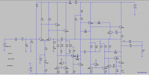
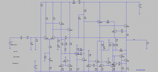
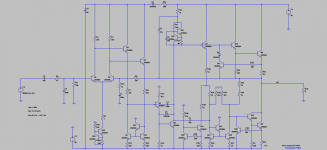
Q13 is called a buffered current mirror and R27+R28 are adjusted so that Vc on Q5 and Q10 match and therefore V(R7) and V(R11).
Clamping the bases of Q8 and Q9 (with LEDs) does not limit the current in Q7 and Q11, resulting in driver failures. This is similar to the classic mistake of clamping the driver bases which leads to VAS overcurrent and failure in more typical amps. The usual solution is to add a third current limit for the vas. I like to bring the negative current limit all the way back to the vas but that can cause stability problems during current limit.
C2 has to be at least 33uF to be effective down to about 20Hz. 47nF is way too small and only provides a bootstrap above about 12KHz.
Connecting the collector of Q6 to the collector of Q11 looses another diode drop of output voltage swing, but is one way of preventing Q11 from ever saturating and limiting the peak current in Q6, but I did not see much rail sticking in the simulation so my choice is to optimize the output swing. Loss of voltage swing / output saturation is an issue with lower voltage amps.
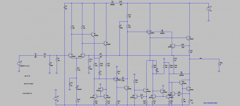
Current mirror circuit
Here is an more refined NPN only amp using a current mirror to drive the lower output.
An issue is the ability to pull the driver output closer to the negative rail than by the current mirror alone, and add a Volt or two to the negative clipping voltage. There are at 3 ways to do this.
1. Add a negative pull down using another bootstrap. This provides the most output voltage because the bootstrap pulls from below the negative rail on peaks. But it requires another large electrolytic cap.
2. Add a low saturation voltage current source. A good solution but requires at least two more transistors.
3. Add a diode to the VAS collector so that the VAS can pull down the driver output. This causes a bit of distortion but only at the peaks where it is small part of the output. This option does not add any load to the driver and is only one more part.
Attachments
I should mention that I have added current limit protection and feedback protecting build-out which could/should be applied to other versions. This version simulates at about 0.0016% THD. Stability of the negative driver is tricky, especially when overdriven, and can be addressed by backing off the OLG which is trade-off.
I'm thinking to call this/these amps my "sow's ear" or "silk purse" amp from the expression about making a silk purse out of a sow's ear.
I'm thinking to call this/these amps my "sow's ear" or "silk purse" amp from the expression about making a silk purse out of a sow's ear.
Last edited:
The diode based circuits tend to have a limit on the THD because the OLG is much different between the negative and the positive half cycles. The vas has to switch into driver mode current to drive the negative output. So the current mirror circuit can out perform the THD of the diode circuit by a factor of ~30.
I should mention that the current source vas pull-up is a good idea because otherwise the diode circuit idle bias is quite sensitive to the supply voltage, ie vas current varies with supply voltage when you just use bootstrapped resistors.
1 or 2 volts of output is a big loss of power for a low voltage amp because power varies as the square of voltage. 10% loss of voltage is 20% loss of power. High saturation voltage loss makes heat worse while the power output is reduced.
Last edited:
Hi steveu
I am having a hard time to control the bias current for the diode version. I think the benefit of the mirror version could not only be the improvement in THD, but because of both half cycles are operating so differently, you need to go in a tradeoff in performance and bias current. My conclusion of I cannot get the bias below 300mA with the diode version, if I want to have some reliable thermal control. (Your second diode circuit had 150mA). So I am about to give up on the diode version.
I am trying to understand the current mirror design a bit better.
- I like the improvement of the two-stage VAS and the good balance on the Q5/Q10 current mirror. I think this balance is essential in achieving a good result.
- R29 (18k resistor at the emitter of the driver of the positive cycle) is affecting the bias current heavily. It looks as the circuit is still very sensitive to this value, which is a bit weird as that resistor is in parallel to a 1k, so it is varying this resistor by few percent only. The bias of the top and bottom power transistor is also not the same. This is a main problem of the npn-only design, I still can't see the output stage is as good as one with complementary transistors.
The assumption is that R24,R25 are a matched pair, as are R27,R28, and the 18K R29 is a bias adjustment which would be about 15K +10K pot in a build. R29 is set so that the Q14,Q15 current mirror detects when Q8 is driven off and drives Q9 on proportionately.
Any imbalance in Q5,Q10 will just create a small output DC offset as the LTP compensates.
For the diode based circuits, the VBE multiplier works the same as in a complimentary circuit. Usually the lower resistor includes a pot because pots corrode and open so you don't want that happening on the top side because that would over bias the output and possibly blow it up. An open pot on the lower side just results in under bias and crossover distortion.
As I mentioned before, the base resistor for the negative output has to be small enough to prevent negative output until the positive side is almost off, ie until the diode starts conducting. 120 Ohms is too much, it should be about 47 Ohms. I realize that reducing this resistor makes the crossover distortion worse, but that's the price of a cool running amp.
A problem with any diode circuit is the speed of the crossover because the whole global feedback loop has to react, vs a normal quasi circuit where the local loop is only the PNP driver and output.
Could it be something as simple as this?
Hi Diego! TotemPole - Sugden. Tube design.
For the Diode circuit - I have tried out a number of VAS stage designs. As you said the positive cycle operates in voltage mode while the lower operates in current mode, and that is an essential problem. But the performance at the crossover is not good, except with excessive bias which was my final result with previous solutions. The current mirror is a nice step forward. Hopefully it is possible to "invest" parts (preferably transistors) to make adjustment of the crossover more easy, or even without adjustments?
The whole npn-only circuit is as perfect as it could be until the VAS. I see no drawback compared to complementary circuits until that point.
The current mirror is extremely sensitive to R17/23 - few ohms and behavior is totally different. The setting of R29 (crossover positive to negative) is not easy to do, and it is depending on the supply voltage. The adding of R27/28 to avoid the driver current jump is also pretty sensitive, but I guess that can be skipped.
The whole npn-only circuit is as perfect as it could be until the VAS. I see no drawback compared to complementary circuits until that point.
Can you enlighten me where you would put the current source please. I think, it would be a very useful simplification. And where would you have put the negative bootstrap, as I believe the negative cycle is in current mode?2. Add a low saturation voltage current source. A good solution but requires at least two more transistors.
The current mirror is extremely sensitive to R17/23 - few ohms and behavior is totally different. The setting of R29 (crossover positive to negative) is not easy to do, and it is depending on the supply voltage. The adding of R27/28 to avoid the driver current jump is also pretty sensitive, but I guess that can be skipped.
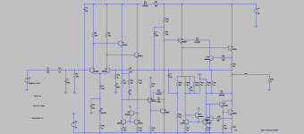
bootstrapped and current source
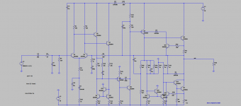
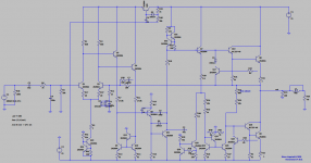
Here is the npn circuit with a driver bootstrap and with a driver current source. I played with the driver current mirror on one to illustrate bias tweaking options. A real circuit would use a pot instead of the small series resistor.
I also remove one of the RC gain boosts because it seems I am pushing the OLG too much.
Note the simulation is driven to clipping to illustrate the clipping levels, ie not for THD estimates.
Attachments
Last edited:
Steve: Yes that is now becoming pretty awesome.
If I simulate at 0.75Vin 20kHz I get some crossover disturbance. If increasing C8 to 100p it is better but some oscillations come up. Therefore I remove C8 and put a 47pF cap between the collectors of Q11 and Q14 (just like on an earlier version). The value of this cap influences crossover from positive to negative cycle, it makes it more smooth. Together with below mirror circuit change the problem is gone.
I modified:
- current source 2mA at the differential (identical performance)
- bootstrap of Q7, replace by current source (2mA) (identical performance and no electrolytic anymore)
- RC R18/C5 not needed (more harm than good I think)
- R27/28 can be removed, they just add an identical offset on both sides of the current mirror. Of course re-tuning is required. R24=R25 =1k is pretty good. R24/25 is slightly dependent on voltage supply but so slightly just leave it 1k. I see no need for a trimpot.
- Value of R17/23 is so important. 10 ohm is somehow ok, 20 Ohm is worse, 1 ohm is good, at 20 mA load.
- I replace the current mirror with the "four transistor Wilson mirror" and this is really performing well in this circuit. For once that this thing makes a sense let's use it.
I did not understand the purpose of the following components
- Removed D1
- Shorted D4
- Shorted R19
I will put them back if I understand why.
I cannot find much other to improve. As perfect as it can ever be. Please comment.
Attachments
The very fact valve based amplifiers are still used and acclaimed by people who are very keen about music, is an indicator, bijunction transistors will continue to be produced. The manufacturer may change but some business person may start producing them. This happened with valves, there is no reason why bijunction transistors have to be an exception.
Remember people, there is a market law which states, if there is demand, someone will try to meet that demand.
Remember people, there is a market law which states, if there is demand, someone will try to meet that demand.
Last edited:
bijunction transistors will continue to be produced
Agree. For sure that is not the motivation for this npn-only design.
However until now there was NO push-pull amplifier without complementary transistors, that was not relying on coupling transformers or electrolytics.
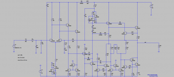
R27/28 move the common mode range of the current mirror down to cover the negative rail. If you remove them the output will clip sooner on the negative side.
D1 clamps Q9 from saturating and causing rail sticking. If you remove R27/28 then you will never get that close to the negative rail anyway.
D4 prevents the the need for the VAS to drive R33 through forward biased CB of Q17. This can happen on negative swings.
R19 moves the pole from Q20 down so that the feedback between Q19/20 is guaranteed stable. An alternate is adding a ~10nF cap across Q20 CE.
The improved current mirror is probably a good idea but there is some danger that the voltage on the collector of Q25 can not go low enough to turn off Q13/Q9.
driving Q8 off
Ah , so there are two ways to address the high frequency cross-over problem.
XX Use diodes to drive Q8 off.
XY Use a separate driver for the current mirror.
Ah , so there are two ways to address the high frequency cross-over problem.
XX Use diodes to drive Q8 off.
XY Use a separate driver for the current mirror.
Attachments
I'm thinking to call this/these amps my "sow's ear" or "silk purse" amp from the expression about making a silk purse out of a sow's ear.
May I suggest sow's ear. It is more audio.
I did remove C5/R17. For the rest my only suggestion would be a NTC driver to pull down the idle bias on heat. I think this will be a very good amp.
Attachments
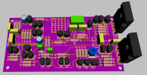
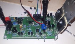
It is working
So I have done a build of the amp with the emitter follower solution (ci-XY). Some small modifications from my side but essentially the same circuit.
The current mirror does not work when using 1k resistors for R24/R25. Transistors keep dying like flies (mirror and driver) and the current at 32mA is too high ( I used 800mA rated BC337). Maybe the transistors get overloaded at startup. I put R24/R25 on 10k and removed the R41/R44 2k bias - after this, no more problems.
Also there was zero bias current. Therefore, instead of two "matched" 1k resistors, I use two 10k resistors, and in series one 1k fix and one 2k Trimpot, respectively. So with the trimpot in mid position the values would match but you can adjust in both directions. (I had to put it on 360 Ohm to get some 100mA bias in cold condition).
Capacitor C2 (47p) has to be removed. It creates instability - it oscillated at 20MHz 1Vpp.
My transistor choice is a bit poor. BC546B, BC337-40 where it takes more current including drivers, BD245C for the output. I run it with a +-15V regulated supply.
The good part:
IT WORKS!
Only npn, no things like coupling caps, transformers, optocouplers,...
What is still open:
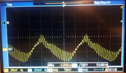
Stability needs improvement. Generally there is an instability thad I already observed before the build. Only at 0.65V 20kHz, never at lower or higher amplitudes. Only visible if you put a resistor (1 Ohm just to trend the current) on Q11 collector. Let´s say slightly visible. You may check it on the last two posted circuits. Not sure how to control these, I tried a lot.
The build is oscillating at 660kHz 600mV, 16MHz 200mV. I just made it work and cpuld try some of the known tricks, however I am very unsure about the source of this instability, and would prefer to tackle it at the source.
Thermal control is missing and bias is drifting rapidly. It increases really fast once it gets a bit hot. For sure a NTC around the Trimpot could do magic but maybe there is a semiconductor solution.
So I have done a build of the amp with the emitter follower solution (ci-XY). Some small modifications from my side but essentially the same circuit.
The current mirror does not work when using 1k resistors for R24/R25. Transistors keep dying like flies (mirror and driver) and the current at 32mA is too high ( I used 800mA rated BC337). Maybe the transistors get overloaded at startup. I put R24/R25 on 10k and removed the R41/R44 2k bias - after this, no more problems.
Also there was zero bias current. Therefore, instead of two "matched" 1k resistors, I use two 10k resistors, and in series one 1k fix and one 2k Trimpot, respectively. So with the trimpot in mid position the values would match but you can adjust in both directions. (I had to put it on 360 Ohm to get some 100mA bias in cold condition).
Capacitor C2 (47p) has to be removed. It creates instability - it oscillated at 20MHz 1Vpp.
My transistor choice is a bit poor. BC546B, BC337-40 where it takes more current including drivers, BD245C for the output. I run it with a +-15V regulated supply.
The good part:
IT WORKS!
Only npn, no things like coupling caps, transformers, optocouplers,...
What is still open:
Stability needs improvement. Generally there is an instability thad I already observed before the build. Only at 0.65V 20kHz, never at lower or higher amplitudes. Only visible if you put a resistor (1 Ohm just to trend the current) on Q11 collector. Let´s say slightly visible. You may check it on the last two posted circuits. Not sure how to control these, I tried a lot.
The build is oscillating at 660kHz 600mV, 16MHz 200mV. I just made it work and cpuld try some of the known tricks, however I am very unsure about the source of this instability, and would prefer to tackle it at the source.
Thermal control is missing and bias is drifting rapidly. It increases really fast once it gets a bit hot. For sure a NTC around the Trimpot could do magic but maybe there is a semiconductor solution.
Attachments
- Home
- Amplifiers
- Solid State
- Amplifier with only 1 type of transistors