... Ian,
I'm really enjoying your input, thank you!
Hugh
Hi Hugh,
I much appreciate your kind comment. Thanks.
BTW TINA-TI has FFT plotting available https://training.ti.com/noise-fourier-analysis-and-signal-chain-content-tina-titm-simulator
KK,
I'll see if I can get your new circuit running using LTspice. Very interesting.
Thanks for posting it.
Cheers,
IanH
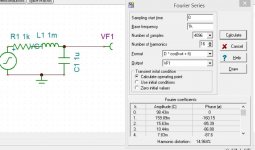
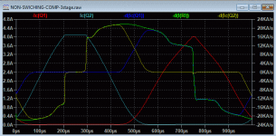
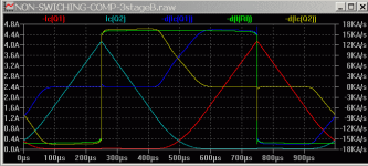
The problem with harmonic distortion measurement is the start delay. Look at the first picture. The LCR low pass 166hz, I pass true it 1khz . If I measure without delay , the LRC shows 15% distortion , and look the phases of the harmonics . Even if I delay 100ms , that is 100 cycles ,still I have a residual distortion but the phases are correct. Ok the graph produced by Tina is worthless as it does not present in logarithmic scale , my be it is the TI free version , but I prefer to work with more precise tools than dandy colorful drawings of LT.
Attachments
Last edited:
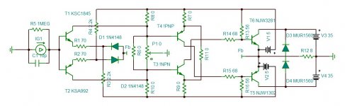
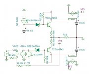
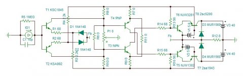
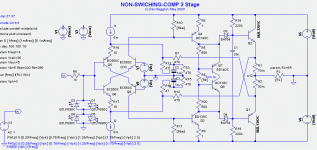
How this circuit should work?
The key feature in this amp is the saturation character of the driver stage.
The outputs are pulled up with resistors for maximum current of 7.5A . As they inherently limit the current .Fly Back diodes are not optional here. The currents of the pull up resistors are swallowed by the drivers except a little amount determined by the collector resistors which biases the outputs.
The drivers at quiescent function in saturation region. In this region the dynamic Hfe ,ic/ib , passes from 100% Hfe unsaturated to 0% fully saturated. My idea is to bias it at 50%Hfe . If so at crossover region where both poles are operating in duo , each sings half loud than each as tenor will sing in solo. All is needed that increase of is exactly decrease of the other . In other words , if one is 75%Hfe the other should be 25%Hfe. In fairy tales as in simulators that can happen , but never in reality. To linearize the crossover , current sense resistors are added to the emitters to convert I to V than a resistor linking the two sense voltages adds up the two , to bring the sum of the currents towards constant.
R6 and P6 adjust the precise 50% operating point for each driver , hence the bias and the offset.
The error input stage could have been a standard double differential. but, by replacing the feedback side transistors with diodes , I got less distortion ,0.15% at 200ua output with twice the voltage gain. Simpler and better.
Hayk.
Attachments
Last edited:
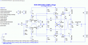
How this circuit should work?
Hayk.
Good work! But R6, R8, R10, R11 can't all be zero?
Did you get non-switching of the output transistors?
Is yours stable with junction temperature for the power transistors?
I had a try to get the circuit in post 39 to work but gave up. I should have used diodes like for your T1 and T2.
Instead I morphed the input stage into one of Lazy Cat's (as used by Andriyol's CFA here). Then to get non-switching I added a Schotky diode in the base of the power transistors - seems OK at 100kHz with a 33nF base-to-base capacitor. It may give you and others some ideas. Files attached.
Notice the circuit has voltage gain.
The ramping d(Ic) means square-laws in the crossover region.
There is a lot of asymmetry causing lots of of 2nd harmonic. Not sure why yet. You or anyone else might like to play with it to get distortion lower
") .
.Attachments
Thank you Ian for the Tina advice. I could figure out how to make it logarithmic as I don't use mouse on my pad. With Tina is possible to input a wave file instead of generator and listen to the sound instead of view on scope. This feature is very important for me.
R=0 means not yet determined.
Hayk
R=0 means not yet determined.
Hayk
Last edited:
R=0 means not yet determined.
Hi kokoriantz,
Ah, thought it might have been some code.
I have likewise used LTspice wav input and save to listen to clipping distortion of some of my simulations. Also to use a short music clip (1 sec) or guitar strum to check average heat dissipation in an amplifier and the transformer VA requirement.
Don't use MJL3281/1302 spice model files . You go no where with such corrupt sim. Onsemi have Pspice , spice2, spice3 models for the NJW 3218/1302 identical transistors but better modeled. Never the less the Hfe's are very high . To get them typical 100 you must modify the parameter BF from 119/100 to 40/25.
Hayk
Hayk
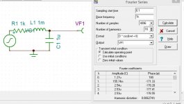
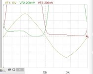
After some 100 cycles, the (start-) step function response has been flattened out leaving the periodic response only, which is more 'harmonic' obviously.You might see an increase reappear when reducing the delay to 10msec.T...that is 100 cycles...
Always more fun with Fourier analysis!
Smart circuitry indeed, the last slightly different from first.How this circuit should work?
What is still not covered are the batteries V1 and V2, and I am curious how inbalance of these 'relative' rails will affect the responses (harmonics, distortion, &c). If these rel-rails are formed from a current source between the power rails, current-mirrored over these p-rails to V1-V2 zeners (or alike circuits), it will make this circuit more complex an prone to various instabilities. Hence the inbalance-sensivity question.
Better use ∞ or oo instead.R=0 means not yet determined.
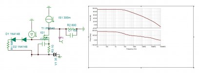
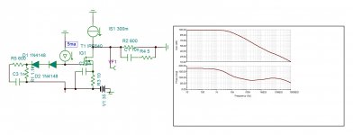
I simulated only the output stage as it is the subject of this thread. Frankly , I love your technique by dividing the base current with fast diodes. Bad mouths will say it is switching diodes, but never both diodes can be cut off as it is current driven. The main problem its nature is high output impedance, makes it current multiplier than voltage follower. The scope is triangle 10khz input 30ma peak . The 220k resistors needs to be bootstraped . Bias=200ma.
I will try this same technique with floating supplies.
By the way for NJWs Hfe modification is wrong . I will review it again , so meanwhile the brave C5200/A1943 are in action
Hayk
I will try this same technique with floating supplies.
By the way for NJWs Hfe modification is wrong . I will review it again , so meanwhile the brave C5200/A1943 are in action
Hayk
Attachments
Last edited:
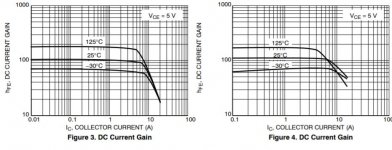
The last decade I used only C5200/1943 BJT . I totaly forgot that other transistors have still low early. Toshiba proudly shows its curves how at currents up to 4A it is flat . It happens that the American ones who by shame hide their curves have even at 200ma a slope curve tripling the Hfe from 5v to 35v. Now if I chose the American ones as NJL3281/1302 because the have constant Ic/Ib transfer function up to 7A, but, on condition that I am running these marvels at a constant 5v , if you please.
So, if they need 5v , I will give 5v. As my floating driver can afford cascode , I can apply any power transistor even multiple paralleled with 0.1 ohm emitter resistors . As the NJL are excellent to 7.5A than 200W @8 ohm is possible , with permissable over 300W @4 .
Attachments
Down the rabbit hole of BJT models
Hi kokoriantz,
You don't need to cascode the output transistors just to get the 5V Vce value of datasheets. If you operate with a Vce fixed at 5V you are in the quasisaturation region and your TINA Gummel Poon model probably does not model quasisaturation. AndyC says here MJL3281A and MJL1302A SPICE Models
Also of concern is the Early effect is not modelled very well as seen in the plot below where just beyond the quasisaturation region where the curve goes linear (around 15V for the 1302) the Early intercept is about 50V but Bob's model uses a VAF of 1000V for the '1302 (571V for the '3281). The reason maybe, as AndyC mentions, to get a good FT fit as Vce varies.
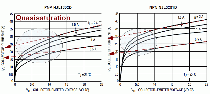
But the LF (DC) Early effect is way too high and this affects the way the Beta (hFE) changes with Vce when the base is current driven as in some circuits in this thread. If the Early voltage is in fact 50V for these devices then the LF Beta will double when the Vce is increased from say 20V to 70V (50V increase)!
But I haven't observed such large Beta increases with Vce change in my current driven CSD amp. It may be that the curves in the datasheets show a low Early voltage due to thermal heating during curve plotting due to insufficiently fast pulse sweeps.
Either way, the datasheets don't seem to be good enough to make accurate models from for power amplifier simulations. And the GP model, even the enhanced one, does not include self-heating, so the Early effect can't be modelled accurately enough for power amplifier simulations that need accurate Beta modelling (such as current driven power transistors).
But we don't need to give up just because our models are not good enough. We can still simulate the basic behavior and compare different ideas. But we can't get reliable information on temperature stability nor accurate information on sound quality of circuits with current driven power transistors..We still need to make them and listen to them.
Hi kokoriantz,
You don't need to cascode the output transistors just to get the 5V Vce value of datasheets. If you operate with a Vce fixed at 5V you are in the quasisaturation region and your TINA Gummel Poon model probably does not model quasisaturation. AndyC says here MJL3281A and MJL1302A SPICE Models
The Cordell models for the '3281/1302 do not use the enhanced GP models quasisaturation. Keantoken has tried using it but not sure if he has released '3281/1302 models with quasisaturation for LTspice.Modern SPICE simulators such as PSPICE and LTspice support the Kull model for quasi-saturation. This is done as an enhancement to the Gummel-Poon model and does not require more advanced models such as VBIC or Mextram.
Also of concern is the Early effect is not modelled very well as seen in the plot below where just beyond the quasisaturation region where the curve goes linear (around 15V for the 1302) the Early intercept is about 50V but Bob's model uses a VAF of 1000V for the '1302 (571V for the '3281). The reason maybe, as AndyC mentions, to get a good FT fit as Vce varies.
But the LF (DC) Early effect is way too high and this affects the way the Beta (hFE) changes with Vce when the base is current driven as in some circuits in this thread. If the Early voltage is in fact 50V for these devices then the LF Beta will double when the Vce is increased from say 20V to 70V (50V increase)!
But I haven't observed such large Beta increases with Vce change in my current driven CSD amp. It may be that the curves in the datasheets show a low Early voltage due to thermal heating during curve plotting due to insufficiently fast pulse sweeps.
Either way, the datasheets don't seem to be good enough to make accurate models from for power amplifier simulations. And the GP model, even the enhanced one, does not include self-heating, so the Early effect can't be modelled accurately enough for power amplifier simulations that need accurate Beta modelling (such as current driven power transistors).
But we don't need to give up just because our models are not good enough. We can still simulate the basic behavior and compare different ideas. But we can't get reliable information on temperature stability nor accurate information on sound quality of circuits with current driven power transistors..We still need to make them and listen to them.
Attachments
The region shown concerns very high currents. If the Datasheet says linear with 5v up to 7.5A it means at this current it did not reach saturation . I have such amplifier with C5200&Co but max4A . I am trying to see the curves of NJWs with xy recorder.
Your amp is excellent , It has 20khz 19vp only 0.8%Dtot. If you NFB by 40db is enough. Your problem is the VAS impedance. The 8 ohm is reflected to VAS as 800 ohms . You need minimum 10nf grounding to get a dominant pole of 20khz. If you are asking this amp 26db gain , than the open loop should be 66db . In other words in open loop 1v input must provoke a votage gain of 2000v . This means the gm of the error and VAS must be more than 2000÷800=2.5S . Actually your Rush error amp has 2× 2mS=4mS dividing the 2.5S means your VAS must have a gain of 625, and this with very very high F pole. What I propose you is something new. Use Wilson mirror , but put 30 mirrors . These are SMD 850C/860C transistors. Thus you get a gain of 30 with no cost as the F pole is above 100Mhz and very low distortion. Now we need 625÷30=21 extra gain . The 10k/470 must be devided by 10to be 1k/47 . This multiplies the gm by 10. The operating current if doubled to 10ma using 2Sc2705/A1145 , it will result the required gm. Now as the current is 10ma , the VAS is running at 300 ma. dissipating over 10W , You need to find an adequate Transistor for it .
Hayk
Attachments
Last edited:
Hi KK,...Your amp is excellent , It has 20khz 19vp only 0.8%Dtot. ...
Thanks. But I stole it from LazyCat
.If the stages are modified for more internal gain it can get 0.07% THD at half output and near 0.001% at 1W. .
Still only 0.5W each in the VAS drivers. 300mA idle. Now little 2nd by changing PNP/NPN emitter resistor ratio.
Attachments
Hi KK,
Thanks. But I stole it from LazyCat
If the stages are modified for more internal gain it can get 0.07% THD at half output and near 0.001% at 1W. .
Still only 0.5W each in the VAS drivers. 300mA idle. Now little 2nd by changing PNP/NPN emitter resistor ratio.
Please do not refer me with k k . You can use my first name Hayk.
The distortion is 0.8%@20khz 19vp is that of your output stage alone in open loop with the Japanese pearls, without bootstrapped pullups. 40db NFB brings this value to 0.008%. I don't think the American ones are suitable for your design.
Last edited:
Hi Hayk,
Re the 0.5 watt driver VAS that's with 15mA. The 300mA idle was for the power transistors. Sorry it was unclear.
I have installed the 2SA1943 and 2SC5200 and got similar distortion (0.11% 19V pk 20kHz). Files attached.
Interesting the 2SA1943 and 2SC5200 models I used have Rs about 50m ohms (Cordell is Rs=0) and Early parameter of 60 volts which seems to be a closer fit to datasheets (Cordell VAF are 1000V and 571V).
So I will continue using the 2SA1943 and 2SC5200 models instead of the Cordell MJL3281 /1302 models. Maybe Bob will update his models?
Sorry for the misnamer, I wasn't sure if your sign off was your name or what.You can use my first name Hayk
Re the 0.5 watt driver VAS that's with 15mA. The 300mA idle was for the power transistors. Sorry it was unclear.
I have installed the 2SA1943 and 2SC5200 and got similar distortion (0.11% 19V pk 20kHz). Files attached.
Interesting the 2SA1943 and 2SC5200 models I used have Rs about 50m ohms (Cordell is Rs=0) and Early parameter of 60 volts which seems to be a closer fit to datasheets (Cordell VAF are 1000V and 571V).
So I will continue using the 2SA1943 and 2SC5200 models instead of the Cordell MJL3281 /1302 models. Maybe Bob will update his models?
Attachments
Goodmorning Ian. Your driver has a load of 800 ohms. To fix the dominant pole at 20khz , you must ground the collectors with 10nf. The maximum slew rate is Imax/10nf. You will need 2× 0.3ma to get 60V/us. This Why the drivers should be mid power transistors of min 40w to dissipate a continues 10w. I suggest you IRF640/IRFP640. At 300ma biased , it gives 93db*+6db VAS gain with Dtot of 0.0077% (mostly to be subtracted by the other pole ) at 20khz 18v p. My output bias is 180ma. Why MJLs and not NJWs , not baptized by saint Bob ? For C5200&Co , use latest model from Toshiba 2017 version . Re =12m.
Hayk
Hayk
Attachments
Last edited:
As I mentioned in #48, middle part.What kind of floating supply you would propose?
A good temp-stable cs (prefer the Sony jfet-bjt combo) say 5mA, mirror both legs over the highest power rails to a suitable value (1:1 - 1:3) and let these currents flow through 5.1 or 5.6 zeners (minimum temp drift) to and from the output. A bjt buffer might be necessary if to much current is drawn or dumped on these relative rails.
Following this topic, and the not-switching claims - and proofs (?), and now also all the extra floating / relative constant voltages needed, it reminds me or better invokes memories of various new class A circuits, with the same aim and corresponding non-switching results. I cannot remember a circuit equal or almost equal as discussed here, but still, lots of ghost from the past swirl around my head. As if this already exist, though, yet not exactly.
Given the nature of the push-pull topology, it is inevitible that measures has to be taken to prevent switching (-off) being a workaround or sufficient overall feedback (if open loop gain permits), or accept inefficient higher bias current up to a safe value, but still an ample (in daily use) of 1A or more.
For me, these 'adjustment' strategies applied to historically based designs, doesn't feel to be the right approach to find a real different solution. After looking at amplifier circuits for some fourty years, only two designers came up with (radical) alternative solutions, and both not 'economic': Pass and Hiraga.
Or switch to class D, the digital world.
Keep on sparring with IanH and see where it leads to.
- Status
- This old topic is closed. If you want to reopen this topic, contact a moderator using the "Report Post" button.
- Home
- Amplifiers
- Solid State
- Non-switching complimentary output stage