The last circuit I posted is intended to provide the same transfer function as shown as the class A in post 129, except that it dissipates less than 50W instead of over 200w. This type of circuit is only 3 days old , the joint problems need to be solved giving all the time it requires . I am interested only with the nonlinear version , as it is not of any concern to others , I will develop it on my own. Once I have reached a final tested result , I'll post it after depositing a copyright .
Hayk
Hayk
Hi Hayk,
BTW the Common Base drive article by Malcolm Hawksford (JAES Oct 1989) is available free here (PDF) Transconductance Power Amplifier Systems for Current-Driven Loudspeakers See Figs 3 and 4.
All the best.
BTW the Common Base drive article by Malcolm Hawksford (JAES Oct 1989) is available free here (PDF) Transconductance Power Amplifier Systems for Current-Driven Loudspeakers See Figs 3 and 4.
All the best.
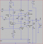
Hello Ian. The real explanition of the circuit is far less romantic than the one you are giving. The starting circuit is the 100w square law
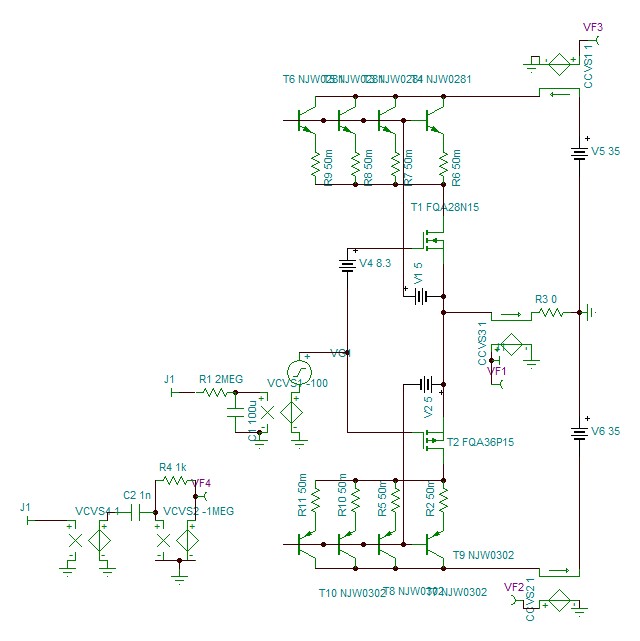
In this circuit there is 2A bias current flowing in the common bases needs to be eliminated. The first approach is to subtract a constant 2A current , and it yields a nonlinear output
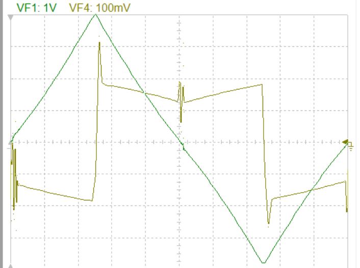
The second approach is to subtract a modulated 2A current and it yields the same as the original character.
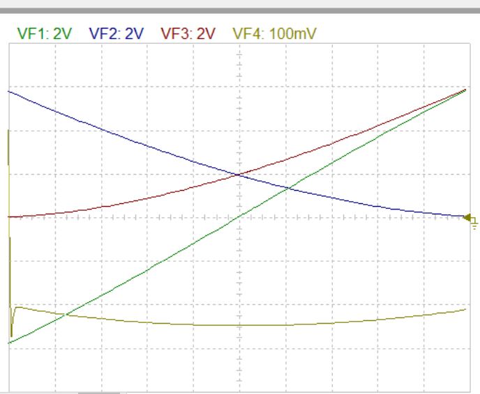
The crossover region in the last case showed accidentally that it doesn't fall to zero or gets doubled but falls to half, which means it can be adjusted to be unity. Whereas of the nonlinear case of my interest , the crossover cannot be a straight line but must be a singular point. I will add an external independent circuit that will subtract or add the at this region about +/- 20ma, to perfect the transition point.
In this circuit there is 2A bias current flowing in the common bases needs to be eliminated. The first approach is to subtract a constant 2A current , and it yields a nonlinear output
The second approach is to subtract a modulated 2A current and it yields the same as the original character.
The crossover region in the last case showed accidentally that it doesn't fall to zero or gets doubled but falls to half, which means it can be adjusted to be unity. Whereas of the nonlinear case of my interest , the crossover cannot be a straight line but must be a singular point. I will add an external independent circuit that will subtract or add the at this region about +/- 20ma, to perfect the transition point.
Last edited:
I will add an external independent circuit that will subtract or add the at this region about +/- 20ma, to perfect the transition point.
Why external? you might be able to use this push-pull modification. Check the currents through R6 and R12 against the output transistor emitter currents. The voltage drops across R6 and R12 are a form of negative feedback signal.
It is a modification of an old Class AB circuit - I used this purely for to illustrate the modification.
Attachments
I don't have LT. Can you post please the circuit picture?
Attachment shows the processing cell for example. The cell resembles a pair interconnected common base amplifiers in one sense of +/-dc low input impedance source inputs. An interesting thought might be to include some high speed op.amps.
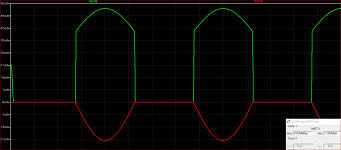
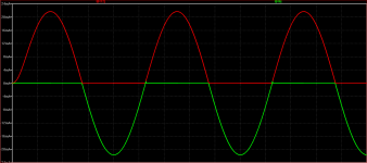
The output is 25V into 8R at 20kHz. The THD is modest however the circuit can re tune the FFT structure to a more monotonic form at that expense.
Attachments
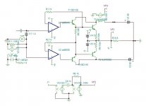
No, I built the RCA circuit in 1981 and subsequently changed the bootstrap collector load on the Vas to a constant current load.
This circuit did use the form of output stage shown in mine but the front end was different. I wanted to explore the output stage as I was planning to built a Leach Low TIM amplifier - which I ended up doing.
The RCA circuit - see attached - makes use of capacitor networks - note the combination R9 and C7 connection for the emitter of the Vas transistor. I seem to remember Nelson Pass using that in a DIY Class A power amplifier.
I am not convinced about the idea of non-switching amplifiers based around BJT devices. Trans-conductance plots follow a curve in the turn-on region, and it is best to avoid locating the switch-on at a point on a curve where the incline in an angle is steep.
If a BJT is not turned off the changed starting point will be higher up on the curve.
Then, when one looks down at the time base on the lateral plane, one sees that narrows the range and time dimensions. This impacts on the Vbe multiplier which has to keep within the range over a range of temperatures for optimum bias.
The Leach amplifier has a very good system to keep heat under control. The heat-sinks they were relatively cool compared to anything else I have built - and all of them were rated for lower power outputs.
The changes I made to my 1991 circuit for non-switching deliver a little less good THD results than the unmodified version. The values I selected for the cell components could be changed - I have changed R12 to 1k36 improve the symmetry, but that made no difference to THD.
There are other ways to improve power amplifier performance like current dumping and Class S due to Sandman which Linsley-Hood analysed in his book on "Valve&Transistor Audio Amplifiers".
Attachments
Last edited:
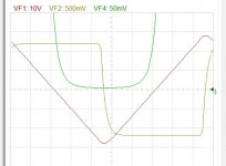
This version gives a non-switching with very low distortion 0.016% @65w 10khz. The foating supply is less than 10ma. If it gives perfect crossover with 350ma bias, but loaded due to Early character of the outputs it is 150ma that gives the lowest distortion. The 10m ohm resistors symbolizes the unevitable wiring resistances.
I applied this output stage in an extraordinary amplifier, that I'll post it in few , it delivers 0.0003% @60w 10khz.
Hayk
Attachments
Last edited:
- Status
- This old topic is closed. If you want to reopen this topic, contact a moderator using the "Report Post" button.
- Home
- Amplifiers
- Solid State
- Non-switching complimentary output stage