Greetings,
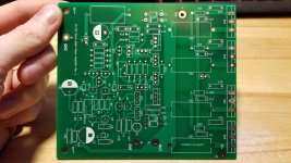
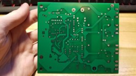
This is my first solid-state power amp project (though I've built a few tube amps). I'm not going to pretend like this is a "groundbreaking" design- it's heavily based off the works of Douglas Self and (especially) Bob Cordell. I figured it would be best to start off with something "normal". After simulations, I committed the huge sin of going straight to a PCB layout, with the expectation that there would be a second revision. Images of my layout as well as a schematic are attached. You can see that there are some extra footprints on the PCB- I wanted to make sure that I had places for caps that might be needed.
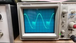
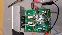
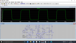
To make a long story short, I have so far been unable to stabilize this thing. It's particularly bad into capacitive loads, as expected. The attached image shows an oscillation that occurs once the amplifier output exceeds something like 22 volts peak. This occurs into resistive, capacitive and open loads. Currently it is running off of +/- 34 V rails from my bench supply, which is current limited to 4 amps. In this case, the IPS, VAS and output stage are all running off the same rails (that's the orange wires in the photo). Note that the emitter resistors on the outputs are actually 0.47 ohms, not 0.22, simply because of what was on hand.
The Zobel network and output inductor aren't shown on the schematic. The Zobel network consists of a 10 ohm resistor and a .1 uF capacitor. The output inductor is of unknown value and is in parallel with a 3 ohm resistor.
C19 and C20 (which are in place of D1 and D2 on the board) made things a lot better, and C16 seemed to help some as well.
Here's a list of things that I tried that didn't help:
-470pF miller caps on the drivers and outputs
-33pF cap in parallel with R10 (unsurprisingly, it made things worse)
-Eliminated the pre-driver transistors and connected the bases of the drivers to the bias spreader with 4.7 ohm resistors (obviously the bias spreader had to change for that). Surprisingly, this didn't seem to help much, if at all.
-Second Zobel network after the output inductor.
Increasing the size of the miller cap C4 does eventually help, but at that point the slew rate is noticeably below 10V/uS. I'd like to see it better than that.
At this point, I'm starting to think that it must be a bad layout or major schematic error, since none of the things I've tried have solved the problem. I'd greatly appreciate some input from those with more experience dealing with this kind of thing.
This is my first solid-state power amp project (though I've built a few tube amps). I'm not going to pretend like this is a "groundbreaking" design- it's heavily based off the works of Douglas Self and (especially) Bob Cordell. I figured it would be best to start off with something "normal". After simulations, I committed the huge sin of going straight to a PCB layout, with the expectation that there would be a second revision. Images of my layout as well as a schematic are attached. You can see that there are some extra footprints on the PCB- I wanted to make sure that I had places for caps that might be needed.
To make a long story short, I have so far been unable to stabilize this thing. It's particularly bad into capacitive loads, as expected. The attached image shows an oscillation that occurs once the amplifier output exceeds something like 22 volts peak. This occurs into resistive, capacitive and open loads. Currently it is running off of +/- 34 V rails from my bench supply, which is current limited to 4 amps. In this case, the IPS, VAS and output stage are all running off the same rails (that's the orange wires in the photo). Note that the emitter resistors on the outputs are actually 0.47 ohms, not 0.22, simply because of what was on hand.
The Zobel network and output inductor aren't shown on the schematic. The Zobel network consists of a 10 ohm resistor and a .1 uF capacitor. The output inductor is of unknown value and is in parallel with a 3 ohm resistor.
C19 and C20 (which are in place of D1 and D2 on the board) made things a lot better, and C16 seemed to help some as well.
Here's a list of things that I tried that didn't help:
-470pF miller caps on the drivers and outputs
-33pF cap in parallel with R10 (unsurprisingly, it made things worse)
-Eliminated the pre-driver transistors and connected the bases of the drivers to the bias spreader with 4.7 ohm resistors (obviously the bias spreader had to change for that). Surprisingly, this didn't seem to help much, if at all.
-Second Zobel network after the output inductor.
Increasing the size of the miller cap C4 does eventually help, but at that point the slew rate is noticeably below 10V/uS. I'd like to see it better than that.
At this point, I'm starting to think that it must be a bad layout or major schematic error, since none of the things I've tried have solved the problem. I'd greatly appreciate some input from those with more experience dealing with this kind of thing.
Attachments
You will need to reveal your design if you want advice, this is the kicker.......
HD
Helps to hit the upload button!
Edit: Just noticed that the drivers are still labeled as being KSC1381 and KSC3503. That is a mistake, they are BD139 and BD140 like the VAS transistors.
Attachments
Last edited:
I would make a few changes to the VAS.
First, remove the cascode BD139 in this section and replace the 139 with a C3503 with low Cob. I would take the collector from the driver C1845 to ground via a 10k resistor and a 330R resistor from emitter to negative ground. This ties the base of the VAS to negative rail and sets at least 2mA plus a few uA through the C185, rather than running only very low base current which highly drives transconductance and loop gain to high levels.
I am guessing now, but I would then decrease Miller cap fropm 100pF across base to collector of the new C3503 to 68pF, and add a phase lead of 15pF from VAS collector to the base of the fb transistor.
This will bring back loop gain, improve stability of the amp, and increase intrinsic linearity before applying fb.
HD
Your output Ground goes to Input.Separate Out Ground and put it between power capacitors.
The photos are a bit deceiving. The ground connection near the output is tied to the PS ground. The other ground connection is just an extra that I'm using as a test equipment ground connection at the moment (blue wire).
Where's the Boucherot cell?
Mike
External, at least during testing. It's the ugly thing you see near the output terminals.
The photos are a bit deceiving. The ground connection near the output is tied to the PS ground. The other ground connection is just an extra that I'm using as a test equipment ground connection at the moment (blue wire).
Thats the thing.The blue wire is signal ground and u should leave it there and then u take another separeted wire only for speaker return and take it directly to PS ground,dont connect this wire on your amplifer board.Your signal ground on board is clean ground and your speaker return wire is dirty ground if u know what i mean.
Last edited:
External, at least during testing. It's the ugly thing you see near the output terminals.
OK...I was looking at the schematic, I didn't notice it in the picture.
Mike
Also Boucherot cell and Zobel should be on that dirty ground.Thats the thing.The blue wire is signal ground and u should leave it there and then u take another separeted wire only for speaker return and take it directly to PS ground,dont connect this wire on your amplifer board.Your signal ground on board is clean ground and your speaker return wire is dirty ground if u know what i mean.
I would make a few changes to the VAS.
First, remove the cascode BD139 in this section and replace the 139 with a C3503 with low Cob. I would take the collector from the driver C1845 to ground via a 10k resistor and a 330R resistor from emitter to negative ground. This ties the base of the VAS to negative rail and sets at least 2mA plus a few uA through the C185, rather than running only very low base current which highly drives transconductance and loop gain to high levels.
I am guessing now, but I would then decrease Miller cap from 100pF across base to collector of the new C3503 to 68pF, and add a phase lead of 15pF from VAS collector to the base of the fb transistor.
This will bring back loop gain, improve stability of the amp, and increase intrinsic linearity before applying fb.
HD
Thanks, I'll take a look at applying those suggestions. Yeah, I've been prototyping with BD139s and BD140s despite their shortcomings since they're cheap and I've certainly blown up a few drivers through some boneheaded mistakes.
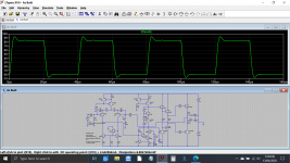
I've been testing with a linear regulated bench power supply for all this, and I wanted to ensure that this wasn't an interaction between the amplifier and the power supply. The amplifier still broke out into oscillation, only this time it was considerably more violent- 9 amps (!). How the outputs survived I will never know, but it took out the drivers, pre-drivers and a VAS transistor. Once replaced, the amplifier was noticeably better behaved (ugh... inconsistencies). As of right now, with a 15 pF cap in parallel with the feedback resistor, it is stable into 100 nF and above caps, though it shows a tiny bit of parasitic oscillation when driven to it's full output swing- not good. a 10 nF cap makes it oscillate with an almost perfectly clean sine wave around 1.5 MHz- cleaner than my function generator is at that frequency
 Fortunately, it doesn't cause the amplifier to self-destruct, so it's a little easier to troubleshoot.
Hopefully your suggestions help with some of these issues, particularly the inconsistencies. I will be doing a second revision of the PCB regardless, since I need to add the footprints for the Zobel network and output inductor. Suggestions for improving the layout are welcome- I've done a few layouts before this, but I am far from experienced with them. I tried to keep the ground connections as low impedance as I could, and I made sure to have as many .1uF bypass caps as possible. I also tried to minimize the loop area with the power devices, though I'm going to try and improve that in the revision- a few extra mm of PCB width is worth it for better performance.
Basi, I do not think that the grounding setup here is the cause of the instability issues because it will oscillate without a load connected. All of the grounding scheme changes once it gets put in a chassis. The main reason there is a ground connection near the input connector is for grounding the shield on the input cable. Obviously the signal ground needs to be referenced to the PS ground, but I see what you are saying about keeping the signal ground quiet- that's the plan, but again, I highly doubt that is causing this particular issue.
Looking at your schematic I would suggest bypassing R10 with about 100pf or perhaps a bit more.
As frequency increases, so does phase shift, until at some point you've built an oscillator ... reducing the upper frequency gain somewhat usually avoids this.
You may also find that you need a low pass filter consisting of a small value series inductor and shunting capacitor on your output leads. This is commonly called a Zobel network and it serves to deal with reactive backload from speakers and crossover networks.
Last edited:
C19 and C20 (which are in place of D1 and D2 on the board) made things a lot better, and C16 seemed to help some as well.
I believe C16 needs to go to the driver -ve rail, not the output section -ve rail. Its value shouldn't need to be that big, try 47pF.
The first thing to try to improve stability is increasing the Miller cap, C4.
Check the bias current - under bias often causes problem.
Q9 collector should go to ground perhaps with a resistor load (decoupled to the -ve rail). That will make its BC capacitance far more linear/constant. ie its an emitter follower, not a darlington first stage.
Not sure what R6 is for, not seen a resistor in that position.
Try 100 ohm base stopper resistors in series with the bases of Q16 and 17 for the same reason you have them in the output trannies .
You may also need a 1K ohm base stopper in series with Q3 base . I have had oscillation from this form of current source although the oscillation was less intrusive , the oscillation was at 112Mhz and was hiding in the output at a low level .
You may also need a 1K ohm base stopper in series with Q3 base . I have had oscillation from this form of current source although the oscillation was less intrusive , the oscillation was at 112Mhz and was hiding in the output at a low level .
As you wrote, you did SIM as I did.
For sine wave signals I got 0.001% THD in 10KHz what is good value. But if I start to test square wave I found oscilation in falling bord of square wave with a strong over voltage oscillation.
For me it means there is compensation issue in this circuit.
I think it is a good pratice to assembly and test amplifier before go PCB layout. I save some money and help to find lots of small issues. Lots of amplifier projects fail because it.
Try to add a polarization resistor in emiter of your Q9 and change your compensation arragement.
Regards
Last edited:
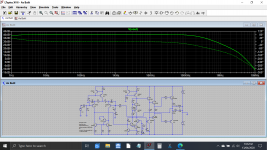
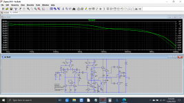
I altered one of my 'Blameless' sims if anyone wants a play. I think its all correct but double check...
The 5k input resistor and those 470pF caps need looking at imo. A proper and well defined input impedance would be desirable.
Its not bad though and should be tweak-able.
Mark makes a good point on the bias setting as that does dramatically alter stability margins as can be seen here.
The peaking on the squarewave is when the source impedance is set to 10k.
The 5k input resistor and those 470pF caps need looking at imo. A proper and well defined input impedance would be desirable.
Its not bad though
and should be tweak-able.Mark makes a good point on the bias setting as that does dramatically alter stability margins as can be seen here.
The peaking on the squarewave is when the source impedance is set to 10k.
Attachments
I think it's worth noting that this will be the power stage of an amplifier. It has (relatively) low closed-loop gain and a low input impedance. It will be driven by the op-amps on the input board.
Mark, I did try increasing the miller cap, but by the time the problem goes away the slew rate is unacceptably low, less than 10V/uS.
Bias is set at about 75 mA.
Someone commented on bypassing R10 with a 100pF cap. That makes this amp go ballistic. I have it bypassed with a 15 pF cap, and even that is a little borderline.
I'll give the VAS modifications a shot and see how it works.
- Status
- This old topic is closed. If you want to reopen this topic, contact a moderator using the "Report Post" button.
- Home
- Amplifiers
- Solid State
- New Amplifier Build Stability