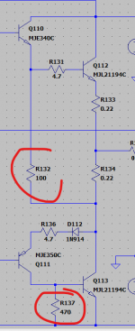
I temporarily have R134 like this (see enclosed). It seems to be helping....
That 100 ohm is really doing the same thing as the two 220 ohms I added.
They very significantly speed up the turn off of the power transistor by removing charge carriers from the junction as well as reducing leakage current of what is really a Darlington pair (driver and output)
Pretty much every amplifier has them in some form or another.
I'm just looking at the TA3200 diagram I had and that shows a 100 ohm for the upper device and a 470 ohm for the lower.
Attachments
Missed a couple of images off the first post:
Mooly,
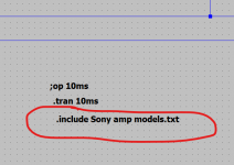
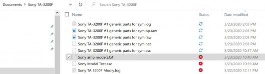
So I added the directive inside my regular asc file, and placed the txt in the same folder. Should I then see added transistor choices when I right click on the pre- or drivers?
If yes, I'm doing something wrong, cause I don't see those added choices. I will persist though.
Stepping back a bit (and as the sym seems to be stable now - right?), I think next step towards troubleshooting is to generate DC readings all over the place, compare with what I'm getting from the live circuit, and interpret. Agreed? As the values I placed on there this far are bare text readings from the live circuit.
If yes, I am not yet sure how the DC readings get generated from the sym file. I added a directive (".op"), but I'm probably missing a step.
Attachments
I think I figured it - at least to read DC OPs, not display them - and it's down in the command bar.
Doing this, I'm trying to verify my actual readings, and the whole area between the collector of Q105 to the base of Q110 (largely reading 0V) seems wrong - should be form 1.6V to 1.8V depending on where you measure. Maybe Q106 is shorted between collector and emitter? I think I should investigate right there.
The working circuit - even with the still off Q choices - shows about 30mV offset at output per sym.
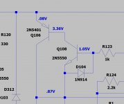
Q106/Q108
Here are some measurements from this trouble spot. Something's totally out of whack there, if you stack it against the sim. The .87V there is the output offset on that channel. The other must have different readings, but just as out of whack. But obviously, no C to E short there. Not sure why I thought of that, frankly.
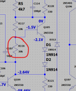
I think one clarifying point out of this simulation work is that the differential pair collectors imbalance is confirmed by it, against what the service manual may want you to think. I wonder if they made up those numbers (-62.4V; -62.8V) just to make it look tight...
Here are some measurements from this trouble spot. Something's totally out of whack there, if you stack it against the sim. The .87V there is the output offset on that channel. The other must have different readings, but just as out of whack. But obviously, no C to E short there. Not sure why I thought of that, frankly.
I think one clarifying point out of this simulation work is that the differential pair collectors imbalance is confirmed by it, against what the service manual may want you to think. I wonder if they made up those numbers (-62.4V; -62.8V) just to make it look tight...
Attachments
Last edited:
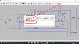
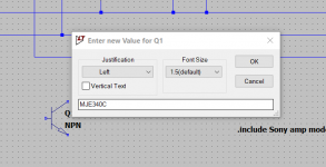
With models added the way I have shown you actually have to go and right click device type and type in the new device exactly as it appears in the model list. So in the image here you right click 'NPN' or whatever device type is already showing.
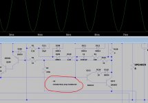
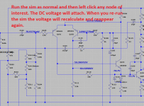
When you run the sim either as a .tran or a .op you can then go and click on any node of interest and the DC voltage will appear.
When you run the sim either as a .tran or a .op you can then go and click on any node of interest and the DC voltage will appear.
Attachments
Make sure the sim is running with a low bias current. I have R117 at 3k and R116 at 40k which is giving about 50 milliamps bias current.
In the real amp the connection between Q106 base and Q108 collector is normally what could be called 'floating' because the transistors are normally off, and so any measurement you make there may not be accurate as it is effectively a floating node.
I would really recommend using a bulb tester on the real amp and perhaps investigate whether there is a problem around the drivers/outputs.
The 0.08 volts on the emitter of Q106 shows the outputs are not biased on. The main amp output is actually more positive than the base drive voltage to the upper driver... so something is amiss. The base of the upper NPN output should be approx 0.6v more positive than the emitter and the same incremental increase should be seen on the base of the NPN driver.
I would force zero bias current by shorting Q105 out from C to E. You should then see zero volts across each output emitter resistor.
If there is doubt over the protection circuitry then you can remove Q106 and Q107 as long as you are limiting the current (bulb tester).
You cant just blame the LTP for a fault.
The problem with an amplifier is its a closed loop system so the problem could be anywhere in the loop. Not saying it isnt the front end, but could be further on.
I would be checking every resistor value. Check all transistor for correct type and do a diode check on them. Didoes can fail too.
I had an amp doing a similar thing and someone before me had fitted an npn instead of a pnp ! what a pig to find as it diode checked ok just the wrong the way around.
Last edited:
You cant just blame the LTP for a fault.
The problem with an amplifier is its a closed loop system so the problem could be anywhere in the loop. Not saying it isnt the front end, but could be further on.
I would be checking every resistor value. Check all transistor for correct type and do a diode check on them. Didoes can fail too.
I had an amp doing a similar thing and someone before me had fitted an npn instead of a pnp ! what a pig to find as it diode checked ok just the wrong the way around.
Agreed with you, Nigel (first paragraph).
Also, after my replacement desoldering machine is delivered (Friday), I may endeavor on a more systematic check of all parts. I find it fascinating though, and a worthy skill to learn and enhance, to hone into the bad part by collecting DC readings, waveform readings, etc. and comparing them to the Spice model. This is really neat.
Been checking resistors last night but can't yet find anything glaringly wrong. Plan to finish resistors soon and when all have one leg out will be easier to test the junctions on the transistors.
On the bulb tester. I am aware of it being used to prevent shorted components from flipping breakers or fuses and stuff, but not sure how it's useful for testing the outputs. Run the amp with the bulb in series and examine the 0.5ohm resistors for anything wildly different, indicating an opened or shorted junction on the finals?
Thank you all your for continued support.
The bulb just limits current and so it can save outputs from blowing if something unexpected happens.
The key is the filaments positive temperature coefficient.
As long as the amp draws little current then the filament is cool and has a low resistance. That allows nearly full mains to be applied to the transformer. If the current rises then the filament heats and its resistance increases dramatically thus limiting the voltage the mains transformer sees.
The bulb just limits current and so it can save outputs from blowing if something unexpected happens.
Cool, got that. Was aware of what the bulb rig does, just not entirely sure how to employ it to my ends in this specific scenario.
I've been working closely on this for longer sessions - having all this time in my hands... - and here some new information I have to put forth:
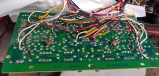
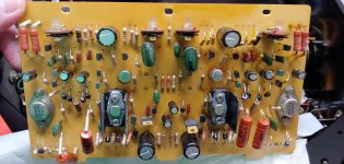
- I came to believe someone (prior to my ownership, of course) spilled coffee on this or something of that nature. I kind of thought what I'm seeing in the amp may be leaking caps, or aging PCB, but there was a thick sludge of sorts. It took a lot of work, but I managed to remove it pretty well. See pics enclosed for sparkly clean PCB.
- Having one resistor leg out, I though, what the heck, let's just replace all resistors with known quantities like my faves CMF55/RN55 and such. This is also because it didn't make a lot of sense to wash the old resistors of the sludge till I got so sweat left and them no markings on. It was that bad. Also, fresh, well done soldering counts for something.
- I did junction tests on most transistors - most prominently, the finals - and got to strikes. Everything seems to be in good shape this far.
From such extensive rework - I don't usually rebuild vintage components to this extent - I expect it to just work when I put it back together (fresh parts, fresh solder joints, checks on everything). If it doesn't, I'm going to re-examine everything, and probably re-run Spice it with exact parts used and see if I get stable operation.
Still, a bit stumped and hope somethings pans out and I have it running again fully.
Thanks all for feedback.
Attachments
Spillage is an ever present problem, something we dealt with regularly in our service dept. For boards like those I would simply wash them in hot water with detergent and then dry.
Stuff comes up looking like new doing that.
Post #10 here:
Washing an amplifier board
So is it for the rebuild
Stuff comes up looking like new doing that.
Post #10 here:
Washing an amplifier board
So is it
for the rebuild So is it
Thank you, Mooly, very much! You've been so helpful.
You can see the sludge somewhat in my initial pics (it was worse than it looks). There was crud under the driver transistors, and in some spots I had to scrape it off with a flat screwdriver. As you can see in my last picture, it looks like new now. What you're describing about washing them off makes a lot of sense. I've just used a combination of pure isopropyl alcohol and flux cleaner (both spray cans). In my case, I am a bit worried the shape of the trim resistors (after the spilling and washing), but I have replacements for those too (I couldn't find the exact physical configuration, so a bit of surgery and "art installation" work will be needed; at least, they're new and encapsulated). Also, cleaned pretty thoroughly the trace side too, as it was full of darkened flux and other dirties. Both sides look pretty handsome now.
I also know I have at least a couple of suggested troubleshooting steps from you, if things are still hairy I will go ahead with them. I didn't have a dim bulb fixture before - I put one together and finally my prairie style outdoor light fixture I've been waiting for three years to install outside my house is put at good use
Also, I have 2N5401s on the inputs, I am a bit in a bind about the values I should use for R309, R310 (as a reminder, they are 220ohms in my amp, while the SM calls for 100ohms. I'm thinking this is to accommodate the odd choices for the actual transistors used on the inputs of my amp). This is where I see LTSpice coming in handy. I will look at your Spice circuit for pointers.
I have not replaced other transistors yet.
Last edited:
I should also say - through this work, painfully contorted at times, I've dearly missed better hardware assembly, like in the case of McIntosh or HK - plug in cards, that is. So, so, soooo much easier to work on. I could have gotten to this point in a fifth of the time, at worst, with a tenth of the sweat and aggravation.
Those open skeleton type presets could be troublesome it is true, not so much by washing but just age... typically any rivets or 'pressed' connections can become a bit flaky and intermittent. Definitely worth replacing as you suggest.
The 220 vs 100 ohm are not critical. All they do is form potential divider with the 47k feeding them, and then the small voltage developed across the 220 ohm is used as a reference voltage for the offset null pot.
So if the offset can be trimmed using 100 ohm then that's fine. If the offset needs more range (preset at one end) then the 100 ohm is increased. If you make the value to large then the preset becomes to critical and finicky to adjust accurately.
So just see what happens and act accordingly.
Make sure you set the bias current (new preset) to the end that gives minimum bias current.
On your sim if the bias preset is R116 then you need that set to maximum resistance value to give minimum bias current. So if it was a 20k preset it would be set to 20k and not 0 ohms.
That is also where the bulb tester saves the day. Get that preset wrong without a limiter and it could be goodnight Vienna, with the bulb and you would just light the room up... and no damage hopefully.
Attachments
Oh, well, literally no change. R117 and R217 still have no effect on the bias adjustment, and DC offset is unchanged at output.
I'm switching my focus to the protection board. From other reports, it's pretty troublesome. It seems to me disconnecting the wires going to R140/R240 takes it out of the circuit. Thoughts?
I'm switching my focus to the protection board. From other reports, it's pretty troublesome. It seems to me disconnecting the wires going to R140/R240 takes it out of the circuit. Thoughts?
57 volts is nearly rail voltage so that suggests that voltage checks should show where the 'loop' is breaking down and something drastic occurring.
Do we have a diagram showing the parts you are taking out?
For the channel with the high offset it might be worth you just copying the LT diagram and marking the voltages you actually see. Something should stand out doing that.
Do we have a diagram showing the parts you are taking out?
For the channel with the high offset it might be worth you just copying the LT diagram and marking the voltages you actually see. Something should stand out doing that.
57 volts is nearly rail voltage so that suggests that voltage checks should show where the 'loop' is breaking down and something drastic occurring.
Do we have a diagram showing the parts you are taking out?
For the channel with the high offset it might be worth you just copying the LT diagram and marking the voltages you actually see. Something should stand out doing that.
Mooly,
Yes, the speaker protection board was clamping down this condition. Once out of the circuit, all this has surfaced.
FYI - the speaker protection board is of the second iteration (Figure 5.4 in the early service manual).
Will be able to investigate this closer later in the day/eve... I'm in home schooling duty with my 6 yrs old. Math time!
- Status
- This old topic is closed. If you want to reopen this topic, contact a moderator using the "Report Post" button.
- Home
- Amplifiers
- Solid State
- Sony TA-3200F: huge output DC offset