Hi people
This is something I've been working on for a while.
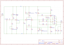
I've written up some more detailed thoughts here... Single Ended Class A MOSFET Current Amplifier - lechaudio
Let me know what you think.
This is something I've been working on for a while.
I've written up some more detailed thoughts here... Single Ended Class A MOSFET Current Amplifier - lechaudio
Let me know what you think.
Attachments
Thanks. I'll have a look, and update.C4 and C5 should definitely go to the supply rather than ground. You may now blow up the whole circuit when the supply rises too quickly, and even if it doesn't, this is bad for the PSRR.
Also, there is room for a turn-on delay, which I'll probably do with a relay, shorting the low-side of the output capacitor to ground.
Last edited:
Which capacitor do you mean?
The R6 shunt between C9-C12 and GND is a placeholder for a relay + a small circuit to prevent thumps. But not to be confused with your earlier comment.
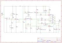
Updated schematic. (I can't seem to add it to the first post because of a 30min timeout, so I'll add it here for now)
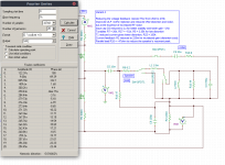
Also, noise results from TINA. Take it with a grain of salt because the PSU is still unknown.
Also, noise results from TINA. Take it with a grain of salt because the PSU is still unknown.
Attachments
Locked in, waiting for parts
Update:
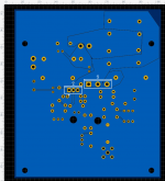
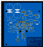
Version 1.0 of the PCB is locked in!")
Now I'm just waiting for parts to come in. My first PCB in a while, so I may be a bit rusty.
I'm a bit apprehensive about all the known unknowns and the unknown unknowns that might go wrong. But also really looking forward to soldering and hearing it for the first time!
I settled on a low-cost CPU cooler, with a PWM controlled 90mm fan
Sigor IV PWM | CPU Coolers | Products | Spire Corp - Powered by Innovation
If all goes well, the TO-247 and T0-220 packages will be a snug fit, and the heatsink won't require too many mods.
Update:
Version 1.0 of the PCB is locked in!
Now I'm just waiting for parts to come in. My first PCB in a while, so I may be a bit rusty.
I'm a bit apprehensive about all the known unknowns and the unknown unknowns that might go wrong. But also really looking forward to soldering and hearing it for the first time!
I settled on a low-cost CPU cooler, with a PWM controlled 90mm fan
Sigor IV PWM | CPU Coolers | Products | Spire Corp - Powered by Innovation
If all goes well, the TO-247 and T0-220 packages will be a snug fit, and the heatsink won't require too many mods.
Attachments
The R6 shunt between C9-C12 and GND is a placeholder for a relay + a small circuit to prevent thumps. But not to be confused with your earlier comment.
Is the amplifier stable with a hard short at the output, no very low frequency oscillations due to the huge capacitive load? Otherwise you may get a thump that depends on where in the oscillation cycle the amplifier is when the relay turns off.
Is the amplifier stable with a hard short at the output, no very low frequency oscillations due to the huge capacitive load? Otherwise you may get a thump that depends on where in the oscillation cycle the amplifier is when the relay turns off.
Only the earthed side of the output capacitor is shorted, so the voltage feedback should still be operational.
I was unable to induce any visible ringing on TINA's oscilloscope by un/shorting the output, even with a 1Hz square wave input signal.
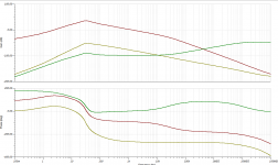
When the output is shorted to ground, there is a sensitivity peak (top curve: common drain V-out), but it looks 1st-order-ish. With declining frequency, voltage feedback is progressively shorted to ground with an RC time constant of about 0.22s (470k × 470n), but looks OK if the input capacitor is kept in check.
Parts should be coming in, so I'll finally be able to build it and find out.
Attachments
Hi
This is not current feedback per se; rather, by referencing the bottom of the feedback loop to the speaker current-sense resistor, the feedback is partially cancelled and output impedance can be higher, like a tube amp. Damping will be reduced with R16 in play.You can add a sitch across it and hear what difference it makes.
Many older amps had variable damping but the modern expectation is for the PA to behave like a voltage source, with zero Z-out and infinite current available.
Am a little puzzled by a couple things --
- what does the emitter-follower, Q6, accomplish and why have it outside the feedback loop? the input impedance of the differential pair is already fairly high
- why use a 1200V transistor, $7(US) and 10A, kind of high for a 20V rail?
But it will be interesting-sounding -- even though it'll be very different with different speaker loads.
Cheers
Replace POT1 and POT2 with a single POT between R7 and R8?
Lose R3 and make POT3 500 ohms?
Is the complexity around POT4 useful? Again I don't think so.
C4/C5 prevent the constant current source from functioning at AC - why?
Your MOSFETs have no gate oxide protection. a couple of zeners might be useful there.
Lose R3 and make POT3 500 ohms?
Is the complexity around POT4 useful? Again I don't think so.
C4/C5 prevent the constant current source from functioning at AC - why?
Your MOSFETs have no gate oxide protection. a couple of zeners might be useful there.
Hi
This is not current feedback per se; rather, by referencing the bottom of the feedback loop to the speaker current-sense resistor, the feedback is partially cancelled and output impedance can be higher, like a tube amp. Damping will be reduced with R16 in play.You can add a sitch across it and hear what difference it makes.
Many older amps had variable damping but the modern expectation is for the PA to behave like a voltage source, with zero Z-out and infinite current available.
I haven't mapped out the exact output impedance vs frequency, but the large value of C7 (470n~2u) should dominate over the voltage feedback (470k) for most of the audio band. The current feedback could be bypassed, but that's the main thing I want to test.
I missed it in the schematic, but in the sim I added 47 ohm in parallel to the speaker, which was a clean way to reduce the resonance peak without increasing distortion, and will put an upper limit on the output impedance.
Am a little puzzled by a couple things --
- what does the emitter-follower, Q6, accomplish and why have it outside the feedback loop? the input impedance of the differential pair is already fairly high
- why use a 1200V transistor, $7(US) and 10A, kind of high for a 20V rail?
But it will be interesting-sounding -- even though it'll be very different with different speaker loads.
Cheers
An input buffer to help balance the long-tailed pair. The RHS transistor has a lot of base current in reserve because of the feedback capacitor, while the LHS relies on the source impedance. It can go without, but then the trimmers may have to be re-tuned if the source is changed.
The Rohm device is a SiCFET with low gate charge, and nice looking linearity so I thought I'd try it. At 2A and likely 70-100°C operating point, the overhead will drop a bit, and it's one of the smallest ones they had that allowed an external heatsink.
Replace POT1 and POT2 with a single POT between R7 and R8?
Lose R3 and make POT3 500 ohms?
Is the complexity around POT4 useful? Again I don't think so.
C4/C5 prevent the constant current source from functioning at AC - why?
Your MOSFETs have no gate oxide protection. a couple of zeners might be useful there.
It may be a bit overkill but I wanted maximum flexibility with the pots. At the input, I can control the bias voltage and current independently. POT3 is the most 'touchy' in the simulator, and I didn't want it to be a source of noise. The CCS needs at least 2-3k ohm to keep the BJT from getting too hot, and I discovered there was also some possible cancellation of distortion with higher values up to 50k.
C4/C5 actually seem to reduce AC ripple in the sense resistor.
Reverse transfer capacitance from Drain to Gate causes the P-channel to switch on a bit more if Vdrain is pulled lower, and vice versa. That mechanism causes ripple in the sense resistor, which the CCS then senses and tries to correct. C4/C5 bypasses that.
I forgot about zeners, so I'll see how badly they're needed and adjust if necessary.
Last edited:
You can use a 10- or 11-turn cermet trimmer for any sensitive positions, much more control.
Or put another way the small signal transistors in the CCS are trying to correct for the shortcomings of the pFET, but only if you remove those decoupling capacitors will that happen at signal frequencies.
That's exactly my point: why stop the CCS from working at AC? The current changes in the sense resistor are real, representing a failure of the CCS to keep current constant, so let it function and the signal across the sense resistor should be reduced signalling good current regulation in the face of the audio signal.Reverse transfer capacitance from Drain to Gate causes the P-channel to switch on a bit more if Vdrain is pulled lower, and vice versa. That mechanism causes ripple in the sense resistor, which the CCS then senses and tries to correct. C4/C5 bypasses that.
Or put another way the small signal transistors in the CCS are trying to correct for the shortcomings of the pFET, but only if you remove those decoupling capacitors will that happen at signal frequencies.
You can use a 10- or 11-turn cermet trimmer for any sensitive positions, much more control.
That's exactly my point: why stop the CCS from working at AC? The current changes in the sense resistor are real, representing a failure of the CCS to keep current constant, so let it function and the signal across the sense resistor should be reduced signalling good current regulation in the face of the audio signal.
Or put another way the small signal transistors in the CCS are trying to correct for the shortcomings of the pFET, but only if you remove those decoupling capacitors will that happen at signal frequencies.
The CCS only needs the right DC level for 2A, and stabilizing the gate voltage directly should be faster than waiting for the error to travel back through the CCS.
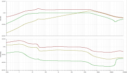
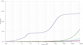
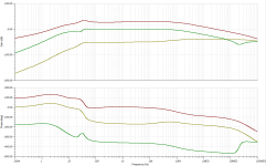
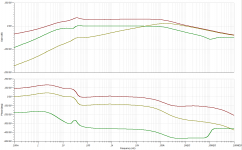
I've attached a screenshot with and without the 10u cap. With the cap it actually has better rejection up to the MHz range. I left room for a fast 10n cap, but in the sim the total difference (10u vs 0p) in THD was 0.052% vs 0.050%, so apart from better PSU rejection, it might not make much or any audible difference.
Red = Vout
Green = Speaker sense resistor
Amber = ripple across the 0.39 ohm
Attachments
I don't think you understand feedback systems. Any meaningful "delay" in the feedback loop could cause oscillation. Feedback starts to act immediately(*), but with a particular frequency/phase response. Small signal transistors are very fast, often upto 100MHz or so,
so there's no reason to suspect any "waiting for the error to travel back", other than phase shifts in the feedback and the amplification network itself.
Slugging a feedback system with too much capacitive load, however, is one way to cause oscillation by swalloing up the phase margin.
The point of the CCS load to the main output device is to reflect the signal current to the speaker, ideally equally across all of the audio frequency range. Any variation across the spectrum will directly affect the frequency response of the system as seen at the speaker.
If the system performs better with the decoupling caps then this means the CCS transistor circuit isn't doing its job and might as well be torn out, or tweaked so it works a lot better. Perhaps it doesn't have enough gain, perhaps it can't drive gate capacitance except at LF only, would need analysing. It sounds as if now its a rather complex DC bias circuit only.
(*) within the limits of the speed of light, so a few nanoseconds at most
Probably not.I don't think you understand feedback systems.
Any meaningful "delay" in the feedback loop could cause oscillation. Feedback starts to act immediately(*), but with a particular frequency/phase response. Small signal transistors are very fast, often upto 100MHz or so,
so there's no reason to suspect any "waiting for the error to travel back", other than phase shifts in the feedback and the amplification network itself.
Slugging a feedback system with too much capacitive load, however, is one way to cause oscillation by swalloing up the phase margin.
The point of the CCS load to the main output device is to reflect the signal current to the speaker, ideally equally across all of the audio frequency range. Any variation across the spectrum will directly affect the frequency response of the system as seen at the speaker.
If the system performs better with the decoupling caps then this means the CCS transistor circuit isn't doing its job and might as well be torn out, or tweaked so it works a lot better. Perhaps it doesn't have enough gain, perhaps it can't drive gate capacitance except at LF only, would need analysing. It sounds as if now its a rather complex DC bias circuit only.
(*) within the limits of the speed of light, so a few nanoseconds at most
Call it lag, then. The parasitic capacitance between gate and drain is unavoidably fast, and nonlinear, so it's better to swamp it with an RC stabilised voltage source, even if there's a little bit of feedback at low frequencies.
- Status
- This old topic is closed. If you want to reopen this topic, contact a moderator using the "Report Post" button.
- Home
- Amplifiers
- Solid State
- Small S.E MOSFET with current feedback scheme -- critique my design