These high voltage chips generally have less bandwidth, are more expensive, and there's no guarantee they will be in production 20 years down the line.
The tripler just needs standard opamps and transistors, and you get to choose performance parameters more flexibly.
The pyramid may be overkill by comparison, but its a general technique that may be of interest.
The input to the drivers just sees a high impedance load - if this reflects significant reactance then you'd probably want to choose high output current opamp(s) with good capacitance driving ability?Yes, driving an OS as in your schematics above, in turn driving a real speaker with challenging crossover.
Some protection resistors are probably wise, but I simulated power-up ramping in the supplies, doesn't misbehave in simulation.Good point about the bootstrap transistors, they're dissipating almost 0.5W each quiescent. Driving the drivers will increase this dissipation.
Is there any way the V+ supply to op-amp could be less than the in/out voltage (vice versa for V- rail)?
TrueA square wave test would be revealing.
There's so much more to consider with a complex design like this and I can't convince myself on first view that this is unconditionally stable. Personally, I've lost many battles to a simple cascode VAS as demonstrated by Self et al. so I appreciate what you're trying to do here.
sorry to drag the meal metaphor along, but the proof of the pudding....
Look forward to hearing more.
")
These high voltage chips generally have less bandwidth, are more expensive, and there's no guarantee they will be in production 20 years down the line.
The tripler just needs standard opamps and transistors, and you get to choose performance parameters more flexibly.
The pyramid may be overkill by comparison, but its a general technique that may be of interest.
Worth it to me for the elegance …..
LTC6090CS8E#PBF Analog Devices | Mouser
Would the decompensated version be OK in the lateral power amp (p21 of datasheet)? Most power amps have gain more than 5 so why not? But I see they specify the LTC0690 not the LTC6090-5 for that amp.
LTC6090CS8E-5#PBF Analog Devices | Mouser Australia
The full power bandwidth of the decompensated version is 65kHz (vs 40kHz. std) on p8 of datasheet.
The schematic below ?
Good question . I would use the LT0690 since I'm not big on slew rate
and go for all the intrinsic stability available .
You would have to try it and see .
Attachments
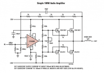

Isn't the gate resistors arrangement a bit unusual for paralleled output mosfets in this schematics?
I would have a 1k at the gate of each output .
AND
Use leds for bias .
Indeed. Might have been a rush job. MOSFET driving impedance looks a bit high in general.Isn't the gate resistors arrangement a bit unusual for paralleled output mosfets in this schematics?
Doesn't take much to drive lateral FETs (as opposed to vertical types)Indeed. Might have been a rush job. MOSFET driving impedance looks a bit high in general.
Doesn't take much to drive lateral FETs (as opposed to vertical types)
See AN-1645 Application Note from TI http://www.ti.com/lit/an/snaa045a/snaa045a.pdf
I can make your life easier -- I still have a tube of LM4702.
Last edited:
See AN-1645 Application Note from TI http://www.ti.com/lit/an/snaa045a/snaa045a.pdf
I can make your life easier -- I still have a tube of LM4702.
As in the middle of this board ?
Attachments
I've been playing with the tripler circuit and reworked it to stop it entering a latch-up state on overload.
Rather than deriving the bootstrap voltage by dividing the tripled output by 1.5, the new version averages the input and output, adding offsets of +/-18V or so. This allows the input to pull the system out of saturation (well in simulation at least).

The response to clipping:

And to square wave input:

V8/V9 and Q3/Q4 act as current source and sink to offset the supply voltages appropriately.
R1/R2/R3/R4 average the input and output and pass to the bootstrap transistors Q1/Q2.
I added a complex load using V5 to modulate the other side of the load resistor.
Connect V6 to input for sine wave testing, V7/V10 provide slew-limited square wave testing.
BTW the distortion is very low of course, 0.001% or so at 1kHz, and the x3 gain section can linearize an output stage well as it has a lot of open-loop gain to spare.
Rather than deriving the bootstrap voltage by dividing the tripled output by 1.5, the new version averages the input and output, adding offsets of +/-18V or so. This allows the input to pull the system out of saturation (well in simulation at least).
The response to clipping:
And to square wave input:
V8/V9 and Q3/Q4 act as current source and sink to offset the supply voltages appropriately.
R1/R2/R3/R4 average the input and output and pass to the bootstrap transistors Q1/Q2.
I added a complex load using V5 to modulate the other side of the load resistor.
Connect V6 to input for sine wave testing, V7/V10 provide slew-limited square wave testing.
BTW the distortion is very low of course, 0.001% or so at 1kHz, and the x3 gain section can linearize an output stage well as it has a lot of open-loop gain to spare.
Attachments
Last edited:
As in the middle of this board ?
The IRF/Vishay MOSFETs need extra drive capability, lateral mosfets not so much.

And just for fun, +/-200V opamp stage
BTW it needs 400V transistors, not the 2N5550/5401's, LTSpice models I used don't seem to model transistor breakdown
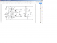
And I suspect it would be tricky to get working for real (and expensive as those kinds of voltages take no prisoners).I've been playing with the improved tripler and turning it into a complete power amp, resulting in two feedback loops around the OS, the tripler stage and a global feedback loop using the first opamp. Seem to be able to get some good results, depends a little on simulation time and tweaking components, but something like:
100Hz: 0.00016%
500Hz: 0.00035%
1kHz: 0.00024%
10kHz: 0.0017%
20kHz: 0.0023% (All with 80kHz BW)
The full-swing bandwidth is only about 50kHz due to the limited slew rate of opamps, but nothing bad happens until the slew limit is hit (about 11V/µs)
Using a 10V amplitude signal on the other end of the 8 ohm load allows reactive loads to be simulated to some extent. 1V amplitide ripple-emulation voltages are added on each rail at different frequencies (to identify them in FFTs).
Here's the 100Hz spectrum:

Note the 1.3V amplitude input signal is amplified x30 to give a 39V (27.6Vrms) output, which is 28.8dB. The spur at 3.5kHz is the emulated reactive load breaking through from the output at about 133dB down. In reality the noise floor would dominate here.
The two opamp feedback loops provide fearsome linearization of the OS, the cross-over harmonics rise to only about 155dB down from the fundamental. Negative feedback doing its job.
Schematic:

The performance at 1kHz is of course a lot worse as each opamp drops 10dB of open loop gain, so 20dB is automatically lost, and cross-over distortion rises with slew rate too, another 10dB down the pan:

And at 10k we are seeing harmonics more clearly:

Also some intermodulation with the 3.5kHz reactive load emulation signal is clear, at multiples of 10k +/- 3.5k - this is because it affects the timing of the zero-crossings. Harmonics are reaching about 95dB down or so.
I haven't added a real OS to my breadboarded version of the tripler yet, its a smallish breadboard, and I've cheated with the bias circuit in this emulation, but I think its promising - emulating a MOSFET OS with this configuration would be fun too.
The hassle of the tripler bootstrap circuitry is repaid by the ability to wrap two nested feedback loops around the OS. The compensation I'm using is rough and ready and definitely an area for research and to investigate in a real implementation.
100Hz: 0.00016%
500Hz: 0.00035%
1kHz: 0.00024%
10kHz: 0.0017%
20kHz: 0.0023% (All with 80kHz BW)
The full-swing bandwidth is only about 50kHz due to the limited slew rate of opamps, but nothing bad happens until the slew limit is hit (about 11V/µs)
Using a 10V amplitude signal on the other end of the 8 ohm load allows reactive loads to be simulated to some extent. 1V amplitide ripple-emulation voltages are added on each rail at different frequencies (to identify them in FFTs).
Here's the 100Hz spectrum:
Note the 1.3V amplitude input signal is amplified x30 to give a 39V (27.6Vrms) output, which is 28.8dB. The spur at 3.5kHz is the emulated reactive load breaking through from the output at about 133dB down. In reality the noise floor would dominate here.
The two opamp feedback loops provide fearsome linearization of the OS, the cross-over harmonics rise to only about 155dB down from the fundamental. Negative feedback doing its job.
Schematic:
The performance at 1kHz is of course a lot worse as each opamp drops 10dB of open loop gain, so 20dB is automatically lost, and cross-over distortion rises with slew rate too, another 10dB down the pan:
And at 10k we are seeing harmonics more clearly:
Also some intermodulation with the 3.5kHz reactive load emulation signal is clear, at multiples of 10k +/- 3.5k - this is because it affects the timing of the zero-crossings. Harmonics are reaching about 95dB down or so.
I haven't added a real OS to my breadboarded version of the tripler yet, its a smallish breadboard, and I've cheated with the bias circuit in this emulation, but I think its promising - emulating a MOSFET OS with this configuration would be fun too.
The hassle of the tripler bootstrap circuitry is repaid by the ability to wrap two nested feedback loops around the OS. The compensation I'm using is rough and ready and definitely an area for research and to investigate in a real implementation.
Attachments
One thing to note is all the discrete transistors operate as current sources/sinks or emitter followers at signal amplitudes, so noise performance isn't an issue and transistor choice should be pretty undemanding.
The first opamp should be the performance defining part, its noise and linearity at moderate gains are important. With low source impedance the current noise of the first opamp isn't particularly problematic either, allowing more choice from bipolar devices.
The first opamp should be the performance defining part, its noise and linearity at moderate gains are important. With low source impedance the current noise of the first opamp isn't particularly problematic either, allowing more choice from bipolar devices.
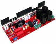
I'm now building up PCB with the opamp tripler circuit, and a separate PCB with its output stage. Waiting for a few more parts (I managed to cook the little trimmer - the large SMT electrolytics need a lot more soak time than I'm used to I think, so the middle of the board slightly over-cooked.
I also forgot to stock up on DIP NE5534A's.
Here's the board part-populated before the oven:

And after reflow:

The circuit is basically as simulated and hopefully in a day or two I'll be starting to commission it. The latest simulation added a bit of bootstrapping to improve voltage swing.
I also forgot to stock up on DIP NE5534A's.
Here's the board part-populated before the oven:
And after reflow:
The circuit is basically as simulated and hopefully in a day or two I'll be starting to commission it. The latest simulation added a bit of bootstrapping to improve voltage swing.

- Status
- This old topic is closed. If you want to reopen this topic, contact a moderator using the "Report Post" button.
- Home
- Amplifiers
- Solid State
- Opamp pyramid stacking for higher voltage operation