Just change the two 10k resistors for 3k3 ones.
Didn't work with the TI Tl071 model I have. What model did you use?
I've been rethinking some bit. If that 33 nF cap across the opamp's supply pins really is crucial for the Current Dumping design, neither the ELEKTOR nor the RCA frontend would work correctly, as both feature a fix and regulated opamp supply and are missing this cap. I'm really curious about the sims.
Best regards!
That capacitor ir far from crucial!
It seems to interact with the the other capacitors in the circuit.
For example, if you rise the two 10pF capacitors to 33pF, then you have to eliminate the 33nF to lower the THD below 0.01% in 10kHz.
Didn't work with the TI Tl071 model I have. What model did you use?
I use any of the two attached.
Attachments
That fixed it. Kinda hard to simulate designs with other OpAmps when fully AC-DC accurate models do not exist.
I built my first current dumping amp in 1977. Copied the Quad 405 design presented in Wireless World. Built Douglas Self's Advanced Pre-amp to go with it. My turntable was a kit presented in Popular Electronics.
I built my first current dumping amp in 1977. Copied the Quad 405 design presented in Wireless World. Built Douglas Self's Advanced Pre-amp to go with it. My turntable was a kit presented in Popular Electronics.
Attachments
It has nothing to do with current dumping, it is just a normal decoupling of the opamp supply.
Did you read any article about the current dumping?
Well, that was exactly your answer to my question
!Best regards!
As the now extinct German electronics magazine ELRAD also published a current dumping amplifier DIY project in the 1980ies, I've read that article including the explanations. But my memory of it is somewhat vague, due to the long time.
So, now tell me, where's that bridge capacitor in the design at the beginning of this thread?
Best regards!
So, now tell me, where's that bridge capacitor in the design at the beginning of this thread?
Best regards!
As the now extinct German electronics magazine ELRAD also published a current dumping amplifier DIY project in the 1980ies, I've read that article including the explanations. But my memory of it is somewhat vague, due to the long time.
So, now tell me, where's that bridge capacitor in the design at the beginning of this thread?
Best regards!
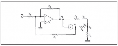
C6, L2, R1 and R17 form the bridge.
I use any of the two attached.
Thank you! They work fine. The TI and ST models do not.
BTW the 33nF cap serves to combine the signals from the two supply pins. You should not assume the crossover that happens in the chip is exactly what you need for the discrete circuit. Better to let that happen at the drivers, otherwise the VAS transistors are operating class AB and not class A.
I am tempted to modify your circuit to eliminate the op-amp. Using an op-amp front end is rarely a good idea. And it distracts form the current dumping purpose of the circuit.
C6, L2, R1 and R17 form the bridge.
Thank you. You're confirming that it's really that cap that I've assumed in #20, but it remains somewhat hard to believe, due to it's tiny capacitance.
Best regards!
Thank you. You're confirming that it's really that cap that I've assumed in #20, but it remains somewhat hard to believe, due to it's tiny capacitance.
Best regards!
QUAD 405 used 120pF.
I am tempted to modify your circuit to eliminate the op-amp. Using an op-amp front end is rarely a good idea. And it distracts form the current dumping purpose of the circuit.
Please try!
I modified the Leach Amp V.4.5 to include current dumping but didn't get good results.
Attachments
but it remains somewhat hard to believe, due to it's tiny capacitance.
Best regards!
As mentioned before, and also as described in the article I linked to, C6, L2, R1 and R17 form the bridge. So the value of C6 is directly related to the value of L2 and the resistor ratios to balance the bridge over frequency. When Xc increases with decreasing frequency, Xl decreases with decreasing frequency and the bridge balance is maintained.
Jan
Edit: one of the authors of the article I linked to above wrote this to me at the time:
Well Jan,
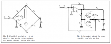
your 405-2 has a number of "enhancements" relative to my older 405. If I label L2 as Z4 (with the parallel resistor!), Z3 as 47R, Z2 as 120pF and Z1 as 500 ohms, then the bridge condition is Z1*Z3=Z2*Z4. I will have to check on the reason for the parallel resistor on Z4. It may be compensating for phase shifts in the drive circuitry. The exact function of C11 is unclear.
Jan
Well Jan,
your 405-2 has a number of "enhancements" relative to my older 405. If I label L2 as Z4 (with the parallel resistor!), Z3 as 47R, Z2 as 120pF and Z1 as 500 ohms, then the bridge condition is Z1*Z3=Z2*Z4. I will have to check on the reason for the parallel resistor on Z4. It may be compensating for phase shifts in the drive circuitry. The exact function of C11 is unclear.
Jan
Attachments
Last edited:
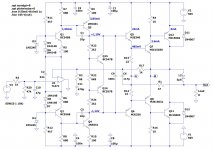
Please help me understand, because I am still in the dark here.After much time simulating the three circuits, the best still is the first one.
Now is the time to order the PCB and do the bench tests.
The balanced bridge, with Z1, Z2, Z3, Z4 .... Which is which?
I understand that Z3 is the 47 ohms in series with the speaker.
Where can I find Z1, Z2, Z4?
... and with R17 being the NFB series resistor, that leaves not much of a choice but C6 as the forth leg of the bridge?I think Z4 is L2. Not sure about the cap (Z2).
Jan
...
And this is the thing that is fuzzy to me. As far as I understand it, the Bridge *MUST* be balanced, or else switching distortion from the current dumper will penetrate further, to the load / speaker.
If aformentioned statement is correct, that would imply that the Balanced Bridge is "not" something that can be negotiable, of fiddled with.
On the other hand, C6 and L2 are in gross violation of my understanding of "balancing" the resistors R17 and R1.
As I understand, such C6 and L2, instead of pure resistances, serve the purpose of tweaking the overall bandwidth characteristics, unity gain margin and phase margin, or at least that is my fuzzy understanding of the matter.
But basically, introducing C6 and L2 results in an *UN*balanced bridge, hence provoking switching noise from the unbalanced current dumpers to penetrate into the load.
So, for my gut feeling, this seems to be a two-edged sword. On the one hand, one strives to tweak the overall gain margin, phase margin, or possibly bandwidth, with these C6 / L2, but on the other hand, the whole concept of a balanced bridge goes down the waste bin.
Or does it????
I am in the dark. Anybody have a light bulb on this?
For me,
47 ohms must be equal 5,6 uH, hence F = XL / 2 / Pi / L = 47 ohms / 2 / Pi / L =~ 1,3 Mhz ...
and
1kohm must be equal 117pF, hence F = 1 / 2 / Pi / Xc / C = 1 / 2 / 3.14 / 1000 / 117pF =~ 1,3 MHz.
So, in a nutshell, what is so magical about the frequency 1,3 MHz ??
Last edited:
- Home
- Amplifiers
- Solid State
- Current Dumping revisited