My guess is that you didn't change the load to 4 Ohms? Attached is two simulations with and without D1 into 4 Ohms.
No, I have use a load of 4 Ω.
My simulation of the original 1970 circuit shows that with or without the D1 diode the negative side of the output voltage is the same.
Maybe some of the transistor or diode models between your circuit and mine are different.
Here is the LTspice file I used. Can you tried?
Attachments
One might expect if such is the case then the FFT of the Class AB design would resemble that for the Class A.
Of course not. That is not what the audio community thinks at that time. This is not how JLH thinks. Read again what he said:
"However, the most careful comparative listening trials, with several of the author's long suffering friends, have failed to uncover any audible difference between these two designs, both of which will almost certainly surpass in performance the best available valve-operated, transformer-coupled units."
In 1970.
Jan
I suggest you look up the preface of "Valve & Transistor Audio Amplifiers" his work published in 1996 for a more considered view on listening panels.
saving Q2?
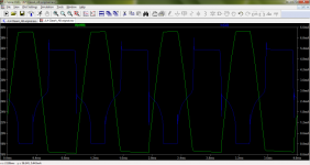
OK here with minimal changes is, with and without D1. Yes, the negative level is almost the same, but the reason is surprising.
Turns out that D1 is a threat to Q2. Modern circuits put a current limit in the VAS transistor to protect it when then the output current limit kicks in. As you can see that when D1 conducts (forward) on the negative limit, Q2 tries to deliver the output instead of Q5. Of course this could easily destroy Q2.
I will attach the slightly modified spice file.
This raises the question, can we do this deliberately instead of adding a pnp driver. I'm going to play with it and get back to you with the results.
No, I have use a load of 4 Ω.
My simulation of the original 1970 circuit shows that with or without the D1 diode the negative side of the output voltage is the same.
Maybe some of the transistor or diode models between your circuit and mine are different.
Here is the LTspice file I used. Can you tried?
OK here with minimal changes is, with and without D1. Yes, the negative level is almost the same, but the reason is surprising.
Turns out that D1 is a threat to Q2. Modern circuits put a current limit in the VAS transistor to protect it when then the output current limit kicks in. As you can see that when D1 conducts (forward) on the negative limit, Q2 tries to deliver the output instead of Q5. Of course this could easily destroy Q2.
I will attach the slightly modified spice file.
This raises the question, can we do this deliberately instead of adding a pnp driver. I'm going to play with it and get back to you with the results.
Attachments
This raises the question, can we do this deliberately instead of adding a pnp driver. I'm going to play with it and get back to you with the results.
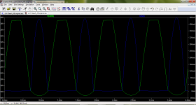
OK, just for fun, here is such a circuit. The VAS is deliberately abused, so it has to be a larger transistor, and, in order to compensate for the lack of negative amplitude, the VAS becomes a Darlington.
The results are actually fair, but nothing short of a complete redesign is going to make this 50 year old amp into a great design. But if you are looking to reuse that old PCB, maybe this is the way to go. Have fun guys.
Attachments
OK here with minimal changes is, with and without D1. Yes, the negative level is almost the same, but the reason is surprising.
Turns out that D1 is a threat to Q2. Modern circuits put a current limit in the VAS transistor to protect it when then the output current limit kicks in. As you can see that when D1 conducts (forward) on the negative limit, Q2 tries to deliver the output instead of Q5. Of course this could easily destroy Q2.
I will attach the slightly modified spice file.
This raises the question, can we do this deliberately instead of adding a pnp driver. I'm going to play with it and get back to you with the results.
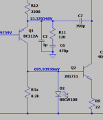
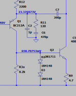
I have looked a simulation of this circuit it clips the current of Q5 with a 1kHz sine wave input of 0.65V and a 4R output load. So the line level sensitivities need adjusting to limit the sources to avoid over- driving the circuit.
If the input voltage is reduced to 0.5V with a 0.1R load at the output Q2 emitter current peak would be about 260 m.A. while the collector voltage varies from 23 to 29.
A quick check of the 2N1711 datasheet suggests these levels are with its' SOA rating.
The zener is necessary - if removed Q4 emitter current will jump from 4.8A to over 9A with the lower input signal and the virtual short.
The point of testing for reliability is to deliberately overdrive the input to determine what could happen, not what should happen. A true reliability test would over drive the input to about 10Vrms, the maximum output a pre-amp might deliver. If we cared, we would test to see what happens when the input transistor E-B junction is driven into avalanche mode.
While many DIYA amps forgo a current limit, that is the function of the Zener. VAS failure due to the activation of the output current limit circuit is a classic design flaw.
None of the 2n1711 data sheets I found actually show a SOA graph but similar 50V/ 500mA devices that show the SOA put the 400mA limit around 13Volts. ie very marginal and since this condition is not well defined, a real hazard. Limiting the VAS current to say 100mA is easy and avoids the problem while maintaining the Zener for the output current limit. Reducing the PNP emitter resistor helps but is not enough to balance the positive and negative current limits.
Last edited:
I suggest you look up the preface of "Valve & Transistor Audio Amplifiers" his work published in 1996 for a more considered view on listening panels.
I prefer what he wrote in 1970. People get smarter all the time

Jan
The point of testing for reliability is to deliberately overdrive the input to determine what could happen, not what should happen. A true reliability test would over drive the input to about 10Vrms, the maximum output a pre-amp might deliver. If we cared, we would test to see what happens when the input transistor E-B junction is driven into avalanche mode.
While many DIYA amps forgo a current limit, that is the function of the Zener. VAS failure due to the activation of the output current limit circuit is a classic design flaw.
None of the 2n1711 data sheets I found actually show a SOA graph but similar 50V/ 500mA devices that show the SOA put the 400mA limit around 13Volts. ie very marginal and since this condition is not well defined, a real hazard. Limiting the VAS current to say 100mA is easy and avoids the problem while maintaining the Zener for the output current limit. Reducing the PNP emitter resistor helps but is not enough to balance the positive and negative current limits.
The data source for 2N1711 was sourced from a 1983 Motorola "Small-Signal Transistor" Handbook which cross references to 2N3019/2N3020/2N3700 for the information on "Active Region Safe Operating Area".
This group is rated for currents up to 1A and it appears to be in current production. The distinction is the capacity to deliver the boosted level of current for periods of 5mS down to 500uS.
The image for the latter is too small to copy off and it seems this has been edited out of On-Semiconductor online datasheets.
There is a .model version of 2N3019 in the standard library for the version of LTSpice I use. If there are doubts about 2N3019 then BD139 or a similar output driver transistor might be considered.
One could also consider adapting the regulated voltage supply with re-entrant short circuit protection to allow enough current for 4R operation.
Also at a control line level one can attenuate the individual sources of input to match the pre-amp peak output levels which the power amplifier can safely handle - the short term capacity with music could exceed that for sine wave output.
I prefer what he wrote in 1970. People get smarter all the time
Jan
I lived through these times and enjoy some looking back to younger adult years ones when life seemed less complicated than nowadays.
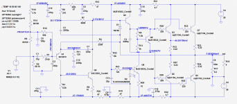
Thank you all for your comments and suggestions so far.
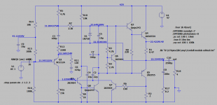
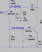
Here is an update of my modifications to the JLH Class AB (1970) power amplifier.
Any other comments or suggestions for improvements are welcome.
regards
George
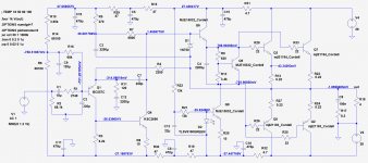
Your compromise solution to the issue raised by steveu in post 44 about the risk of failure of Q4 under output short conditions seems to be the 220R stoppers in the output stage transistor bases.
There is another way to do this since you have included R8 in the emitter connection of Q4 to the negative rail.
Taking advantage of the voltage drop across the 10 Ohms of resistance to activate an additional NPN transistor strapped in between Q4 base and the negative rail then becomes an option.
Thus so, limiting of Q4 current would start when the base emitter voltage of the additional transistor reaches just over 0.5 Volts.
Last edited:
Your compromise solution to the issue raised by steveu in post 44 about the risk of failure of Q4 under output short conditions seems to be the 220R stoppers in the output stage transistor bases.
There is another way to do this since you have included R8 in the emitter connection of Q4 to the negative rail.
My simulations showed that the 220 Ω value at the base of the output transistors were two high and reduced a lot the peak output voltage at 4 Ω.
So I have to redude them at 22 Ω.
I have to replace the Q4 transistor to a KSC2690 type because of the risk of failure of Q4 under output short condition. The new transistor has a much higher Ic (continuous and peak) current.
The updated schematic is shown below.
Attachments
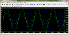
These (attached) illustrate some current limit options for the VAS, not including a simple resistor nor the inclusion of the VAS in the PNP current limit feedback loop. The R9 values are selected for about 100mA limit. The LED option creates a lot of loss but offers a overload indication.
I any case, one EF stage after the VAS is simply not enough current for 4 Ohms, unless you deliberately abuse the VAS and allow it to conduct hundreds of mA. The ratio of the peak speaker current to the VAS current is more than the Beta of a typical (power) transistor, ie 5A/5mA =1000 and only a Darlington transistor has that much current gain.
I should note that the VAS-D1 over-current completely bypasses the PNP outputs so the base blockers are not involved. D1 connects the VAS directly to the (shorted) output.
I know you want to reuse your PCB, but if you are going to invest in a new power supply and new power transistors, hanging on to that old circuit is a dubious choice. A typical "blameless" circuit would make so many problems go away for hardly any more money.
Attachments
I think you don't take into consideration transistor Q6.
The bias current of Q4 is 2.5 mA, the bias current of Q6 is 115 mA.
Suppose that the output is 25V at 4 Ω, the output current is 6.25 A.
So 115/2.5=46 and 6.25 / 0.115=54
I cannot see how you came to the conclusion that a beta of 1000 is required.
Am I missing something?
The bias current of Q4 is 2.5 mA, the bias current of Q6 is 115 mA.
Suppose that the output is 25V at 4 Ω, the output current is 6.25 A.
So 115/2.5=46 and 6.25 / 0.115=54
I cannot see how you came to the conclusion that a beta of 1000 is required.
Am I missing something?
I think you don't take into consideration transistor Q6.
The bias current of Q4 is 2.5 mA, the bias current of Q6 is 115 mA.
Suppose that the output is 25V at 4 Ω, the output current is 6.25 A.
So 115/2.5=46 and 6.25 / 0.115=54
I cannot see how you came to the conclusion that a beta of 1000 is required.
Am I missing something?
Yes, my mistake, the gain of Q6 does help out the PNP as well as the positive output. I had already discounted the circuits with 100mA bias as space heaters. But 115mA is not enough for 4 Ohms. As shown in simulations, the original circuit clips prematurely on the negative side. The boosted supply voltage and two PNPs in parallel may help, but I don't have that file to simulate. Perhaps MJL21193 have that much gain at 3 Amps but a MJ2955 at 6 Amps does not. As a rule of thumb, assume a gain of about 10 at peak currents.
This amp was designed when transistors were expensive and "solid state" was new. It was great for its time but I don't see any reason to live with those constraints 50 years later. Ironically, the dual bootstrap is back for use with MOSFETS due to their ~4 volt vto.
I appreciate your help.
I understand that this is a 50 years amplifier.
I am interested because I have built the JLH Class A design and it was really good except the heat.
According to JLH both amplifiers are acoustically the same but the 1970 design does not produce all this heat.
Here is the LTspice file that I use for the simulations.
regards
George
Attachments
Only two real issues found.
1. Negative rail sticking. This seems to be due to the VAS over current at clipping. A pair of diodes on the VAS base removes the sticking but causes a tiny bit of distortion in normal operation. You may want to do that but I found that making the VAS a Darlington with current limit handles the rail sticking and improves distortion. There is one issue and that is stability due to the feedback from the VAS to the input. I show a 10pF compensation cap to handle this but it's probably not necessary.
2. VBE multiplier resistors. Because the VBE multiplier is conducting ~100mA, the divider network should conduct about 10% of that so that the base current is less than 10% of that, ie Beta > 100, 10% of 10%. This might be a good place for a 2 transistor VBE multiplier.
OK, 3. The base blockers on the power transistors were still too big. These are BJT power transistors driving 4 Ohms so the base blockers should not be much bigger than 4 Ohms.
and 4. I messed with the bootstrap resistors. I can't think of a good reason to portion them the way they were. The main difference is that the bootstrap cap doesn't need to be so big.
and 5. I messed with the input bias to create a temperature stable DC offset. This is only as important as you feel about it.
If you jack up the bias, you can get some impressive THD figures, but you get about 0.015% at 45mA, ie pretty good without a lot of heat. Just tweak the VBE multiplier.
Attachments
Last edited:
When I ran the simulation the maximum unclipped output voltage into 4R test load was 25 peak.
The static current drawn by the output stage was 250 m.A. per pair while that drawn by the driver stage was 120 m.A - so things are warming up.
Transistor current gain in transistor datasheets is specified at room temperature 25 degrees C but it increases in proportion to degrees K where your 25 degrees translates to 298.15.
The output transistors are likely to get warm in which case you should be able to reduce the standing current of the driver stage a little.
MJL3281 and MJL1302 have higher current gain than MJL21194/21193 and for the same purpose these are a viable alternative.
There is quite a lot of diffusion capacitance in the base-emitter junction of a transistor which has some low pass filtering implications.
I would use lower value stopper resistors and try to run the output stage at low dissipation as well as that you have so designed.
Only two real issues found.
1. Negative rail sticking. This seems to be due to the VAS over current at clipping. A pair of diodes on the VAS base removes the sticking but causes a tiny bit of distortion in normal operation. You may want to do that but I found that making the VAS a Darlington with current limit handles the rail sticking and improves distortion. There is one issue and that is stability due to the feedback from the VAS to the input. I show a 10pF compensation cap to handle this but it's probably not necessary.
2. VBE multiplier resistors. Because the VBE multiplier is conducting ~100mA, the divider network should conduct about 10% of that so that the base current is less than 10% of that, ie Beta > 100, 10% of 10%. This might be a good place for a 2 transistor VBE multiplier.
Can you explain what you mean by "Negative rail sticking". I am not sure that I understand what you mean.
Yes, you are correct for the Vbe multiplier. I will check it.
regards
George
- Status
- This old topic is closed. If you want to reopen this topic, contact a moderator using the "Report Post" button.
- Home
- Amplifiers
- Solid State
- Modifications to the JLH 15-20W Class AB amplifier (1970)