Hello, I'm a beginner (kinda) and have been interested in symmetric input and amplification stages for some time.
After reading the The push-pull VAS section on D.Self's book, I tried replicating his design (the one which combines input stage current mirrors with the push-pull vas) on LTSpice and indeed encountered the issues he described (mainly the impossibility of setting the VAS current as it settles by itself at some microamps).
The other issues were: excessive dissipation at the beta-enhance emitter-follower and oscillations due to the lack of current in the VAS (especially if I put a cap across the VBE multiplier).
So I tried a method of forcefully setting the VAS current:
I'll be absolutely honest here: I pulled this circuit out of my ***, but the simulation didn't give me such bad results, so I wanted to know if I should even waste my time prototyping it despite its weirdness. (also because prototyping it will take a loooong time)
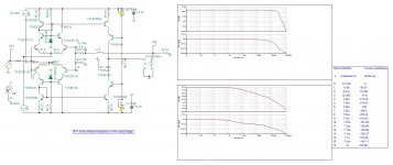
I'm attaching the phase/gain plots, THD measurements and a description, as well as a PDF schematic so you can see the components more clearly. I'm also attaching the .asc file.
I plan to use the same components simulated here except:


Thank you very much.
After reading the The push-pull VAS section on D.Self's book, I tried replicating his design (the one which combines input stage current mirrors with the push-pull vas) on LTSpice and indeed encountered the issues he described (mainly the impossibility of setting the VAS current as it settles by itself at some microamps).
The other issues were: excessive dissipation at the beta-enhance emitter-follower and oscillations due to the lack of current in the VAS (especially if I put a cap across the VBE multiplier).
So I tried a method of forcefully setting the VAS current:
- Driving the base of a current mirror with the signal from the input stage
- Using the transistor not responsible for setting the mirror current as the beta-enhance EF
- And finally, using the voltage across the EF resistor (which is under a constant current) to set the VAS current
I'll be absolutely honest here: I pulled this circuit out of my ***, but the simulation didn't give me such bad results, so I wanted to know if I should even waste my time prototyping it despite its weirdness. (also because prototyping it will take a loooong time)
I'm attaching the phase/gain plots, THD measurements and a description, as well as a PDF schematic so you can see the components more clearly. I'm also attaching the .asc file.
I plan to use the same components simulated here except:
- VBE multiplier: I'll use a 2SC3807 instead of the BD139
- Pre-drivers: I'll use a 2SC3423/2SA1360 instead of the BD139/BD140
- Drivers: I'll use a 2SC5171/2SA1930 instead of the BD139/BD140
Thank you very much.
Attachments
Hi.
There appears to be some "weirdness" in the IPS, but it looks like the drawing is missing loop compensation, which explains the graph. It points toward instability. Try a small cap in series with a resistor (zero), parallel with R55, maybe like 33pf & 150R, and see if phase margin improves.
There appears to be some "weirdness" in the IPS, but it looks like the drawing is missing loop compensation, which explains the graph. It points toward instability. Try a small cap in series with a resistor (zero), parallel with R55, maybe like 33pf & 150R, and see if phase margin improves.

Apply 1GH inductor in series with R55 to have it open loop at ac , then you can see you phase margin at 30db.
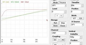
So I went and did that, as you suggested. At 30dB the phase is already at -168°, and at -180° the gain is at 9.2dB, giving 20dB of gain margin but only 12° of phase margin.
But I can't see how that relates to the problem, in closed loop whenever I add any meaningful capacitance in parallel to R55 and look at the plot, the phase never crosses -180° before some dozens of MHz and when it finally does, the gain is already at something like -80dB or less.
Correct me if I'm wrong but that shouldn't oscillate.
If you add a 10k or so collector resistor to the emitter followers they won't fry if something else is wrong (such as VAS transistor goes open).
With push-pull VAS you have two entire amplifiers upto the bias circuit, which is why a single feedback path cannot define operating point. It strikes me one way to address this is to use a single resistor in place of the bias circuit, and use an opamp in differential configuration to compare the voltage across the bias circuit (now static) with the swinging bias resistor's voltage. The feedback at the differential pairs needs a common-mode signal from the amplifier output, summed with a differential-mode signal from the aforementioned bias feedback circuit.
Somepoint I might try simulating such a setup - I suspect the bias circuit can just be a single diode, with the multiplication factor implemented by the relative gain for the two differential signals to the opamp, or by splitting the bias resistor into pieces.
Of course you still have multiple feedback paths, which is the fundamental problem push-pull VAS circuits have, and why they are probably not a good idea!
bit off-topic, but how do you calculate the bypass cap values of C5 and C21 in the pre-driver / driver stages?
The speedup caps? In theory you base them on the stored charge of the devices, their purpose is to drain stored charge from the base of the device that is switching off at the crossover point quickly. I suspect a bit of experimentation is needed, I wouldn't assume device models are particularly accurate for stored charge behaviour. They can be much larger than needed without penalty though I think.
Like letting the VAS current settle itself at those microamps and using an op amp to sense the voltage swing, comparing it with a fixed bias, using that to drive the output stage and taking individual output signals to feed back separately both differential input pairs? Sounds very creative.
I've though of other methods to try making it work as well as found an article D.Self was referring to in his book, it was created by Samuel Groner and published in Jan Didden's Linear Audio. Circuit is shown in Figure 12.
P-P VAS is really interesting despite its many problems, unfortunately (and understandably) people are not very fond of it.
Your method of stabilising the vas current was described by Giovanni Stochino in Electronics World April 1997.
Glad to know someone else did it, my approach to this problem was a complete "what if". I'll try to find this article.
You don't need triple Darlington on the output . Eliminate Q32/33 . The outputs have hfe of above 120 typical, BDs I measure commonly hfe300.
Yes, the original iteration of this circuit, before I applied the spice models, had good THD (0.0025%), no pre-driver and the phase margin was huge (80~90°). But when I inserted the models the driver stage loaded the VAS and THD went up to 0.016% so I chose to use a pre-driver.
Maybe I should try more output stage topologies to try to regain phase margin? Like keeping the pre-driver as an emitter follower and turning the drivers+output pairs into a Sziklai? Not sure how the circuit will respond to these mixed pairing though.
What happens if you leave out C30?
Nothing relevant to the AC path, it's just there to stabilize the voltage across R63 (68k resistor), it may be a little too small for that but I already have 2 LPFs on the rails to smooth the supply ripple going to the small signal section.
For what server R59/60 1k . With cascade VAS , Cherry capacitor feeding from the output rather then Miller C11/12 is superior . See Lm3886.
R59/60 and R17/18 are emitter degeneration resistors for the current mirror that helps setting the VAS current. Furthermore, R17/18 also serve as emitter resistors for the beta-enhance EF that drives the VAS.
I'm not familiar with these advanced compensation techniques but I tried encompassing the entire output section with the miller caps (if that is what Cherry compensation means), now the caps are in parallel with everything from the input stage to the output node, and guess what, the phase margin got smaller but the stability plot still looks ok and I'm finally able to connect small capacitances in parallel with R55. And the THD didn't get worse at all!
Now I've been able to add more than 33pF directly in parallel with R55, as long as I raise the value of the compensation caps accordingly (but the THD starts getting worse and worse). 47pF demands the compensation caps to be bigger than 270pF and the THD starts approaching 0.010%.
I think I'll try changing the output stage to regain phase margin since I tried applying cherry caps to the original iteration of the circuit (the one with ~90° phase margin) and it dealt much better with the parallel capacitance but it was still using ideal transistor models. I may also try different compensation techniques.
But in the end, I may not use anything in parallel with R55 since this "compensation" only introduces more phase shift and oscillation, I just didn't want to build the circuit and it start oscillating because of stray capacitances. Before I put the cherry caps just 2pF in parallel with R55 was enough to make it oscillate.
I can't thank you people enough, really!
You can probably stabilize the circuit be increasing C11 and C12 but of course that slows it down. An alternate solution is to degenerate the input diff-amp(s). The basic problem is that your circuit is too complicated, too many stages in the feedback loop.
And if you do the simulations, you will probably find that symmetrical inputs do not out perform asymmetric inputs. Besides, asymmetry produces even harmonics which are often a deliberate "feature". I recommend an exercise of testing the circuit with and without each feature to discover the benefits/cost of each. This usually leads to something like D Self's "blameless" circuit.
And if you do the simulations, you will probably find that symmetrical inputs do not out perform asymmetric inputs. Besides, asymmetry produces even harmonics which are often a deliberate "feature". I recommend an exercise of testing the circuit with and without each feature to discover the benefits/cost of each. This usually leads to something like D Self's "blameless" circuit.
This is what I did, with same resultAnd if you do the simulations, you will probably find that symmetrical inputs do not out perform asymmetric inputs.
")
This file show up what can be done to improve this old amplifier behavior.
I tried to send also all my support files like models and potentiometer but is not allowed by forum.
I am sure you can work around this missing files and understand all working principle and compensation technics applied.
I like the way you draw your schematics. You did it to all understand well your electronic ideias - congratulations.
Have fun and good times with it.
Ronaldo
Attachments
Last edited:
- Status
- This old topic is closed. If you want to reopen this topic, contact a moderator using the "Report Post" button.
- Home
- Amplifiers
- Solid State
- Push-Pull VAS