Searched for "ABC" , "AB+C", but could not find anything.
Dear All,
Has anybody tried, built, listened to an amplifier that works in class ABC ?
Or more precisely, in class AB + C ?
This would basically mean two paralleled output stages, but with their cross-over points offset by a certain amount of voltage.
Specifically, I am mulling about things I read in this article:
CCDA & Class-AC
(Thank you, John Broskie!).
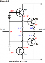
Even more specifically, about this very picture:
https://www.tubecad.com/2009/11/12/class-ac.png
If you look at the bubbles closely, it basically looks like "two paralleled typical AB output stages" ..... but with two series connected bias generators, and a very specific way of connecting the four driver transistors.
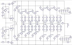
My draft of a possible ABC class output stage looks more or less like this:
Tell me what you think. Any pitfalls here? Pro's? Con's? Do's? Don't's?
The only down side of such an AB+C architecture that I see is that it will not achieve as much peak to peak output signal swing, as in the case of a typical class AB amplifier, with a single cross over area. What am I missing?
Cheers,
Ziggy.
Dear All,
Has anybody tried, built, listened to an amplifier that works in class ABC ?
Or more precisely, in class AB + C ?
This would basically mean two paralleled output stages, but with their cross-over points offset by a certain amount of voltage.
Specifically, I am mulling about things I read in this article:
CCDA & Class-AC
(Thank you, John Broskie!).
Even more specifically, about this very picture:
https://www.tubecad.com/2009/11/12/class-ac.png
If you look at the bubbles closely, it basically looks like "two paralleled typical AB output stages" ..... but with two series connected bias generators, and a very specific way of connecting the four driver transistors.
My draft of a possible ABC class output stage looks more or less like this:
Tell me what you think. Any pitfalls here? Pro's? Con's? Do's? Don't's?
The only down side of such an AB+C architecture that I see is that it will not achieve as much peak to peak output signal swing, as in the case of a typical class AB amplifier, with a single cross over area. What am I missing?
Cheers,
Ziggy.
Attachments
Last edited:
.. two additional comments.
1. Please kindly note that if you are considering to build a typical class AB amp with a typical single cross over region, you would be probably using more than one output transistor pair anyway.
Looking at a class AB with say two pairs, converting it into two sets of single pair output stages does not introduce too much complexity. Apart from the doubled bias generators and additional drivers /pre-drivers.
2. The 'complex' emitter degeneration resistors on my picture are an attempt at addressing anti-gm-doubling, according to a different method. A slightly different approach / subject. Irrelevant for the AB+C discussion at hand.
Last edited:
Class C is used for RF transmitters as it introduces a large amount of harmonics which are filtered out before the aerial or load.
Class C can be used in FM or Class D amplifiers, it is called class D, not class C.
The Yamaha M2, M50 and M70 uses bias on the output transistors to avoid crossover distortion and is not class C, it is class B.
Class C can be used in FM or Class D amplifiers, it is called class D, not class C.
The Yamaha M2, M50 and M70 uses bias on the output transistors to avoid crossover distortion and is not class C, it is class B.
I am generally aware o the conduction angle being substantially less than 180 degrees in Class C. Not sure though, does the 'large amount of harmonics' apply in this particular scenario.Class C is used for RF transmitters as it introduces a large amount of harmonics which are filtered out before the aerial or load.
Class C can be used in FM or Class D amplifiers, it is called class D, not class C.
The Yamaha M2, M50 and M70 uses bias on the output transistors to avoid crossover distortion and is not class C, it is class B.
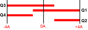
The general idea is to "pair up" the conduction angle of Class C, which is significantly less than 180 degrees, with a conduction angle that is appropriately substantially more than 180 degrees, so as to jointly achieve a seamless "cross-over" .... but not necessarily at the zero-signal point.
Please take a look at the conduction angles of the four transistors within the concept, as depicted:
Transistor Q1 is "paired-up" with transistor Q4. When the one stops conducting, the other takes over.
Similarly,
Transistor Q2 is "paired-up" with transistor Q3. When the one stops conducting, the other takes over.
Both of the aforementioned pairs have their own "cross-over" point.
But both of these points are in a different place, and none of these points coincides with the "zero-signal-crossover" point.
To say more: At the cross-over point of Q1 and Q4, when the transition occurs, the other pair of transistors is in a state of stable continuum, i.e. works so as to "alleviate the ripple". And vice - versa.
Jointly, the four transistors seem to be working in a "constant gm" mode, with no gm doubling in any area: At any point and at any time, it is always exactly two transistors that are conducting.
Does this seem feasible and doable in light of what you wrote earlier, or am I missing something ?
I also attach three graphs from Mr. John Broskie's article ( CCDA & Class-AC ), to better show the two transition points.
Attachments
Last edited:
The article describes this as two class B outputs working in parallel. Why not just use one Class B output?
It looks a bit like the author is trying to solve the gm doubling effect of a class A stage by turning it into two class B stages. Which begs the question why not start with one class B stage?
It looks a bit like the author is trying to solve the gm doubling effect of a class A stage by turning it into two class B stages. Which begs the question why not start with one class B stage?
Please look at the picture with the conduction angles of transistors Q1..Q4 in post #6. Indeed, these are two "Class B" outputs. Working in parallel. But there is a small trick here: each of these "Class B" outputs has its hand-over point at a different place. So at the time when one of the "Class B" outputs is undergoing a hand-over, the other one is within stable conduction of one of the transistors in its pair. In other words, the "Other Class B" unit is under continuous (kink-free) conduction, of quite a healthy current, that may serve to "swamp and hide" any of the "hand-over-artifacts" of the "Class B" unit that is undergoing the handover.The article describes this as two class B outputs working in parallel. Why not just use one Class B output?
It looks a bit like the author is trying to solve the gm doubling effect of a class A stage by turning it into two class B stages. Which begs the question why not start with one class B stage?
"One Class B" stage would have its single hand-over point, and to make it worse, this hand-over point is exactly at the zero-signal crossing.
As the "One Class B" stage will probably have more than one pair of output devices anyway, with the output devices readily available, so why not give this concept a chance?
Many kind thanks for signalling these. Just looking at the schematic of the M2. It seems that indeed Yamaha was using a very similar concept in this model. Frankly speaking, they took it even a step further, in terms of implementation and simplicity.
Many examples of this out in the big bad world Phase linear Amcron Dc300A coming to mind I myself made a no of these in the late 1970 ,s I have still got one upstairs That worked hard for over thirty years
The secret is to get the AB side working for the first 1/2 watt and then bring in the larger C transistors
My design would today be considered old fashioned but at the time I was very pleased with it
Trev
The secret is to get the AB side working for the first 1/2 watt and then bring in the larger C transistors
My design would today be considered old fashioned but at the time I was very pleased with it
Trev
Yes, I did about 7~8 years ago.Has anybody tried, built, listened to an amplifier that works in class ABC ?
Or more precisely, in class AB + C ?
I didn't actually use the extravagance of two actual Class B stages in parallel, instead I used a single stage, and breakpoints provided by diodes and resistors.
Conceptually, the end result is exactly identical, but the cost is halved.
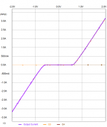
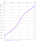
It is possible to obtain quite good results: here are some sim results of that time (one prototype must still be gathering dust somewhere in a crate).
First, the naked OP stage:
Note the two-current slopes characteristic of the AC class, and the THD for the OP alone which is already <0.1%, without FB or anything.
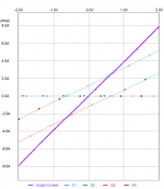
When such a stage is included in a complete amplifier, the THD falls at a (certainly fictional) level comprised between 0 and 10ppb, depending on the evaluation method:
I didn't retain it in the end, because the quiescent current needs to be really high, between 0.25 and 0.5A minimum, which generates a serious amount of heat
Attachments
Kind thanks for your valued inputs.Yes, I did about 7~8 years ago.
I didn't actually use the extravagance of two actual Class B stages in parallel, instead I used a single stage, and breakpoints provided by diodes and resistors.
Conceptually, the end result is exactly identical, but the cost is halved.
It is possible to obtain quite good results: here are some sim results of that time (one prototype must still be gathering dust somewhere in a crate).
First, the naked OP stage:
[...]
Note the two-current slopes characteristic of the AC class, and the THD for the OP alone which is already <0.1%, without FB or anything.
When such a stage is included in a complete amplifier, the THD falls at a (certainly fictional) level comprised between 0 and 10ppb, depending on the evaluation method:
[...]
I didn't retain it in the end, because the quiescent current needs to be really high, between 0.25 and 0.5A minimum, which generates a serious amount of heat
Hey, were those diodes of a normal forward voltage 0,7V, or did you try to use some low Vf schottky types, or something?
My idea for bringing the power dissipation down on such a scenario would be to actually increase the value of the emitter resistors and at the same time - try to find a type of diode that is both quick, but with a low forward voltage at the same time. With a lower Vf, the bias current could be smaller ...
I also noticed that the value of your resistors in the "diode-bearing" branch is significantly LESS than the value of the resistor in the "non-diode-bearing" branch. Is this a result of your Spice simulation optimizations, or did you come to these values by means of some theoretical concept / theory / calculation?
Why are they so ... small ?
As far as **amplifier** Class goes, this is Class AB, period.
The speaker load receives current and voltage during the 360 degree cycle and that´s all that matters.
How is that current achieved internally at the amplifier is irrelevant; calling this Class ABC or AB+C is just semantic pedantry, doubly so because results do not match the label.
If anything, I see a normal Class AB amplifier there, where Class AB transistors are helped/boosted by others during part of the cycle ... so what´s the big deal?
If it were News, then this should be front page headlines :
:

Not the first time I see tubecad "advancing Audio" by doing things the weird way, last week was a preamp with clipping diodes at the output in the best guitar distortion pedal tradition..
Me?
I feel overintelligent/different enough by putting butter on the bottom side of the toast.
The speaker load receives current and voltage during the 360 degree cycle and that´s all that matters.
How is that current achieved internally at the amplifier is irrelevant; calling this Class ABC or AB+C is just semantic pedantry, doubly so because results do not match the label.
If anything, I see a normal Class AB amplifier there, where Class AB transistors are helped/boosted by others during part of the cycle ... so what´s the big deal?
If it were News, then this should be front page headlines
:
Not the first time I see tubecad "advancing Audio" by doing things the weird way, last week was a preamp with clipping diodes at the output in the best guitar distortion pedal tradition..
Me?
I feel overintelligent/different enough by putting butter on the bottom side of the toast.
Class-AB+C is the same thing as Bob Cordell's DoubleCrossTM
Good to see some interest in this. Bob Cordell's 2nd Edition Chapter 13.7,8 has a section on it but Bob calls it "Double Cross(TM)" or Class-DX(TM) -- a definite an improvement on Douglas Self's Class-XD.
Bob made output stages and provides lots of THD results in his book. But not sure if he has built a full amplifier using it yet.
I have simulated it and have a spreadsheet for Bob's Fig 13.8a you can download here
Bob Cordell's Power amplifier book
You can see how to bias to get a wide Class-A near distortion free sweet-spot with no feedback covering the first watt -- amazing! I believe the 1st what is watt really counts in audio, just like Nelson Pass and fiends (sp?).
I also posted a circuit here Has anyone seen Rush pairs used this way? For a CFA with true differential inputs with a Rush driver OPS (with voltage gain which allows lower voltage and lower power fast lower voltage drivers) with current driven power transistors (as described in my Linear Audion Vol.13 "CSD" amp). But this Class-AB+C (Double Cross) version hasn't been built and tested yet. It's there free for others to use for ideas. I developed my Class-AB+C independently of John Broskie and Bob Cordell -- I only found their works after I posted my circuits.
Discussion on Bob's DoubleCross(TM) circuits might be best posted to his book thread - he deserves some feedback having spent so much effort researching and writing it. It's a really good book.
Cheers...
Hi Ziggy,Searched for "ABC" , "AB+C", but could not find anything.
Dear All,
Has anybody tried, built, listened to an amplifier that works in class ABC ?
Or more precisely, in class AB + C ?
This would basically mean two paralleled output stages, but with their cross-over points offset by a certain amount of voltage.
Specifically, I am mulling about things I read in this article:
CCDA & Class-AC
(Thank you, John Broskie!).
Even more specifically, about this very picture:
https://www.tubecad.com/2009/11/12/class-ac.png
If you look at the bubbles closely, it basically looks like "two paralleled typical AB output stages" ..... but with two series connected bias generators, and a very specific way of connecting the four driver transistors.
My draft of a possible ABC class output stage looks more or less like this:
Tell me what you think. Any pitfalls here? Pro's? Con's? Do's? Don't's?
The only down side of such an AB+C architecture that I see is that it will not achieve as much peak to peak output signal swing, as in the case of a typical class AB amplifier, with a single cross over area. What am I missing?
Cheers,
Ziggy.
Good to see some interest in this. Bob Cordell's 2nd Edition Chapter 13.7,8 has a section on it but Bob calls it "Double Cross(TM)" or Class-DX(TM) -- a definite an improvement on Douglas Self's Class-XD.
Bob made output stages and provides lots of THD results in his book. But not sure if he has built a full amplifier using it yet.
I have simulated it and have a spreadsheet for Bob's Fig 13.8a you can download here
Bob Cordell's Power amplifier book
You can see how to bias to get a wide Class-A near distortion free sweet-spot with no feedback covering the first watt -- amazing! I believe the 1st what is watt really counts in audio, just like Nelson Pass and fiends (sp?).
I also posted a circuit here Has anyone seen Rush pairs used this way? For a CFA with true differential inputs with a Rush driver OPS (with voltage gain which allows lower voltage and lower power fast lower voltage drivers) with current driven power transistors (as described in my Linear Audion Vol.13 "CSD" amp). But this Class-AB+C (Double Cross) version hasn't been built and tested yet. It's there free for others to use for ideas. I developed my Class-AB+C independently of John Broskie and Bob Cordell -- I only found their works after I posted my circuits.
Discussion on Bob's DoubleCross(TM) circuits might be best posted to his book thread - he deserves some feedback having spent so much effort researching and writing it. It's a really good book.
Cheers...
WHOAAA !!!!Hi Ziggy,
Good to see some interest in this. Bob Cordell's 2nd Edition Chapter 13.7,8 has a section on it but Bob calls it "Double Cross(TM)" or Class-DX(TM) -- a definite an improvement on Douglas Self's Class-XD.
Bob made output stages and provides lots of THD results in his book. But not sure if he has built a full amplifier using it yet.
I have simulated it and have a spreadsheet for Bob's Fig 13.8a you can download here
Bob Cordell's Power amplifier book
You can see how to bias to get a wide Class-A near distortion free sweet-spot with no feedback covering the first watt -- amazing! I believe the 1st what is watt really counts in audio, just like Nelson Pass and fiends (sp?).
I also posted a circuit here Has anyone seen Rush pairs used this way? For a CFA with true differential inputs with a Rush driver OPS (with voltage gain which allows lower voltage and lower power fast lower voltage drivers) with current driven power transistors (as described in my Linear Audion Vol.13 "CSD" amp). But this Class-AB+C (Double Cross) version hasn't been built and tested yet. It's there free for others to use for ideas. I developed my Class-AB+C independently of John Broskie and Bob Cordell -- I only found their works after I posted my circuits.
Discussion on Bob's DoubleCross(TM) circuits might be best posted to his book thread - he deserves some feedback having spent so much effort researching and writing it. It's a really good book.
Cheers...
Slowly ... I think that I stepped into something deep. Something that overwhelms me. Brain went into clipping.
Anyways, many kind thanks for the eye-opener and links to valuable reads.
Actually, a true honor that you were inclined to notice my posts and mulings.
Got some homework to do. I was kind of hoping do to a practical "AB+C" (or other anti-gm-doubling) gig, with a fairly simple circuit, but it seems the subject is deep water. Deeper, than I can embrace, for the time being.
Will need to obtain 2nd edition of Bob's book and dig into the subject of DoubleCross(TM).
...
As for your CSD driven output stage, with FAST drivers - indeed, beautiful!
The simulation - seems to be very promising. An interesting concept. Interesting, how the practical aspects of stability would turn out in a real life implementation, especially considering the 2:1 gain within the OPS.
Was the "2:1" chosen arbitrarily, simply as a "conservative number" ?
Why not 3:1 or anything else? Pushing ones luck?
...
The Yamaha M70, if I understand the OPS schematic correctly, uses a fairly simple scheme with the 4R7 resistors ladder, but I perceive that solution as not ideal, because it actually results in a different current loading of the output transistors, which is not ... "cool". (Or at least, that is how I understand the circuit).
What I would be searching for, is basically to find a KISS (Keep-It-Simple-And-Stupid) approach/architecture, that implements the two-crossover-points concept, and each of them - not at the zero-signal-crossing point. With equal current loading of the output transistors.
Would be even better, if this quickie KISS solution could be "embedded" with no hassle into the existing architecture of some proven "classical AB" amplifier design. (as the Ovation e-Amp, for example).
Having a bunch of 2sc5200/2sa1943, and 2 x 0,3K/w radiators per channel, I am trying to find a nice idea for building something more than just a "classical AB OPS with paralleled pairs of output devices".
Many kind thanks for your inputs.
Cheers,
Ziggy.
If you look at their type N°, you will see that the diodes of both examples are schottkyKind thanks for your valued inputs.
Hey, were those diodes of a normal forward voltage 0,7V, or did you try to use some low Vf schottky types, or something?
IIRC, I made a crude arithmetic estimation based on fixed voltages (300mV) and no internal resistance which I used in a sim, where I refined the values to take into account various real-life effect: junction equation, ohmic resistance, etc.I also noticed that the value of your resistors in the "diode-bearing" branch is significantly LESS than the value of the resistor in the "non-diode-bearing" branch. Is this a result of your Spice simulation optimizations, or did you come to these values by means of some theoretical concept / theory / calculation?
Why are they so ... small ?
The values ended up rather low for the C branch, because the diodes have a non-negligible resistance of their own
- Status
- This old topic is closed. If you want to reopen this topic, contact a moderator using the "Report Post" button.
- Home
- Amplifiers
- Solid State
- Class AB+C: Anybody tried it? Is it worth it?