This is a very unusual thread as it is really asking for help/expertise and asking whether anyone can spot any possible issues related to problems that have appeared in real world examples of this design. I know that there is some serious expertise on the forum when it comes to design and build of CFA designs, whether you feel you could offer an opinion or make suggestions 'essentially for free' is up to you. It is quite an interesting circuit though.
It is only fair to say right at the start that only the simulation file is offered and that no other details are available. My only connection in all of this is in having been asked to try and help out.
The file has been produced by another technician working on repairing this amplifier and the people involved in the design and production of the amplifier have agreed to the simulation file being discussed. It has become a problem child.
It appears the design has had issues with 'repeatability' and problems have occurred in service. These typically manifest as high frequency instability and under some circumstances hum and buzzing which appear to be related to the times the amplifier is oscillating. The buzzing reduces as the unit warms.
Typically the amplifier may oscillate at power on and although essentially non-destructive it does burn up the 10 ohm in the C/R network across the speaker terminals. This oscillation appears to be in the 300 to 400kHz region and can be picked up on AM radio. This oscillation I believe is in the 16 volt peak region (so I'm assuming over 30 volts across the speaker terminals).
When the amplifier is not oscillating, it can be provoked by simply turning a nearby electrical appliance on/off or by switching from balanced to unbalanced operation. Should the amplifier then burst into oscillation then it seems this is sustained and it can not be stopped unless the power is removed.
There is also a low level higher frequency oscillation (around 5 MHz in the real build) that is visible when the speaker relay is not connected.
The real design seems somewhat critical on semiconductor component types used as fitting different gain groups (for example in the driver stages) changes the nature/frequency of the oscillation but does not provide a fix. Getting the semi's 'right' also seemed to fix the low level hum that some examples had experienced.
(I suspect the hum issue is related to the instability rather than a simple case of hum due to other more mundane reasons)
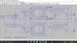
The simulation file should click and run providing you keep the model file in the same folder. The models are for a handful of devices and are from Bob Cordells site.
Under the upper row of output devices are two resistors used to set the bias current. This allows the user to use a lower power option when needed.
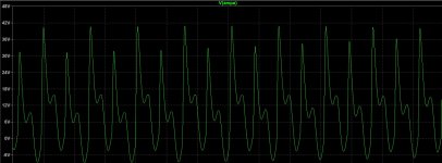
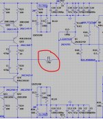
In simulation I have been able to generate very similar looking oscillation to the real world designs by adding a little parasitic inductance (20uH) to the signal feed to Q1 and Q30 base's as shown in the attached image.
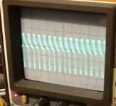
The attached scope shot shows the real problem.
And that is really as far as it has got. Any insight or thoughts that anyone has on this would be welcomed.
It is only fair to say right at the start that only the simulation file is offered and that no other details are available. My only connection in all of this is in having been asked to try and help out.
The file has been produced by another technician working on repairing this amplifier and the people involved in the design and production of the amplifier have agreed to the simulation file being discussed. It has become a problem child.
It appears the design has had issues with 'repeatability' and problems have occurred in service. These typically manifest as high frequency instability and under some circumstances hum and buzzing which appear to be related to the times the amplifier is oscillating. The buzzing reduces as the unit warms.
Typically the amplifier may oscillate at power on and although essentially non-destructive it does burn up the 10 ohm in the C/R network across the speaker terminals. This oscillation appears to be in the 300 to 400kHz region and can be picked up on AM radio. This oscillation I believe is in the 16 volt peak region (so I'm assuming over 30 volts across the speaker terminals).
When the amplifier is not oscillating, it can be provoked by simply turning a nearby electrical appliance on/off or by switching from balanced to unbalanced operation. Should the amplifier then burst into oscillation then it seems this is sustained and it can not be stopped unless the power is removed.
There is also a low level higher frequency oscillation (around 5 MHz in the real build) that is visible when the speaker relay is not connected.
The real design seems somewhat critical on semiconductor component types used as fitting different gain groups (for example in the driver stages) changes the nature/frequency of the oscillation but does not provide a fix. Getting the semi's 'right' also seemed to fix the low level hum that some examples had experienced.
(I suspect the hum issue is related to the instability rather than a simple case of hum due to other more mundane reasons)
The simulation file should click and run providing you keep the model file in the same folder. The models are for a handful of devices and are from Bob Cordells site.
Under the upper row of output devices are two resistors used to set the bias current. This allows the user to use a lower power option when needed.
In simulation I have been able to generate very similar looking oscillation to the real world designs by adding a little parasitic inductance (20uH) to the signal feed to Q1 and Q30 base's as shown in the attached image.
The attached scope shot shows the real problem.
And that is really as far as it has got. Any insight or thoughts that anyone has on this would be welcomed.
Attachments
Realising that not everyone uses LTspice I have attached a PDF of the circuit details.
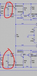
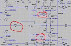
A bit more info that came to light is the circuitry around Q19/R18 seems to have come under scrutiny at some time. The problem amp did not have the 1k fitted, however replacement PCB's did have the part in place. Either board still oscillated though.
I was a little puzzled by those four 15 volt Zeners (2 per amplifier side) as they don't seem to do anything.
Attachments
Realising that not everyone uses LTspice I have attached a PDF of the circuit details.
A bit more info that came to light is the circuitry around Q19/R18 seems to have come under scrutiny at some time. The problem amp did not have the 1k fitted, however replacement PCB's did have the part in place. Either board still oscillated though.
I was a little puzzled by those four 15 volt Zeners (2 per amplifier side) as they don't seem to do anything.
Those two diodes look like some poor's man protection for VAS overcurrent. I don't think they are doing much, though, at 15V across it is likely the VAS devices are already gone.
One thing that drew my attention is the very low current through D1/D2 (slightly over 1mA) for a 6V2 zener. If those diodes are current starved anytime during a steep transition (power on included) then everything is possible.
Some components coices look suspicious. MJE15032/33 for VAS cascoding, that's an open invitation to at least poor performance, if not straight instability.
To be honest, it is almost impossible to follow this schematic, at least in the way it is drawed. Is one transistor Q13 1A transistor biasing both halves in class A, doesn't make much sense? All I can tell is that a 500KHz oscillation strongly correlates with the global feedback loop stability (I can't even spot it right away), since it is closed to what such a high current amplifier with slow transistors (4MHz) ULGF should employ.
Last edited:
Thanks for for taking a look at this. It looks like the sim has used fairly generic models although I see what look like the real choices written on the diagram for some of the devices.
You might have something with your thoughts on the Zeners and those transistors because I believe the behaviour at start up is 'random' and on some occasions it can be OK... more or less... although it can be provoked back into oscillation.
Certainly as drawn it only has one transistor controlling bias currents.
I've attached a sim with the two added 'parasitic' inductors as these give a similar-ish looking instability to the real design and also in the right frequency range. With the amp oscillating like this, nothing I tried really made it stable.
Another suspicion is simply layout and the way the whole amp is constructed. I believe the PCB's are quite 'track intensive' being single sided and with lots of long thin traces. So another worm in the can")
I'll have another look tomorrow.
You might have something with your thoughts on the Zeners and those transistors because I believe the behaviour at start up is 'random' and on some occasions it can be OK... more or less... although it can be provoked back into oscillation.
Certainly as drawn it only has one transistor controlling bias currents.
I've attached a sim with the two added 'parasitic' inductors as these give a similar-ish looking instability to the real design and also in the right frequency range. With the amp oscillating like this, nothing I tried really made it stable.
Another suspicion is simply layout and the way the whole amp is constructed. I believe the PCB's are quite 'track intensive' being single sided and with lots of long thin traces. So another worm in the can
I'll have another look tomorrow.
Attachments
This is an indication for long pcb traces acting as antennas and imho reveals a quite "fishy" design.When the amplifier is not oscillating, it can be provoked by simply turning a nearby electrical appliance on/off or by switching from balanced to unbalanced operation. Should the amplifier then burst into oscillation then it seems this is sustained and it can not be stopped unless the power is removed.
Yes, I believe the board layouts are quite leggy with long thin traces. Good thinking, thanks.
And further sim investigations...
I've tried taking the output stage out of the feedback loop and this resulted in the front end appearing stable, at least as a quick go/no-go result. Next I tried with just the final driver in place (no output devices) and the oscillation returns if I keep the parasitic inductance in place.
I tried slowing the output stage down, first by using alternate models for outputs and driver (2N3055 and TIP41) and that changes things a bit.
I've also tried adding a little series resistance to the final drivers base and also increasing C13 and C23 which are the 100pF caps between C and B of the final drivers. That essentially killed all oscillation in the sim. How the real world amp would react is an unknown at this point though.
Ignoring the parasitic inductance there are two phase shifting parts of the circuit connecting to Q10 collector - lag capacitor C3 at 470pF and Q1 Miller capacitor C13 at 100pF - this arrangement mirrored in the opposite half.
With stability the dominant pole in any system has to be ten times greater than any other pole.
The base voltage swamping resistor you included for Q1 would have given a degree of isolation from the impact of C13 and resulted in a more output for Q1.
If this added resistor was to be increased in value Q1 base to emitter capacitance could be enough for C13 to be reduced in value to the point where the poles are not in conflict or possibly eliminated.
Your observation about use of lower fT components is interesting. The MJE15032/33 transistor fT is about a quarter of the originals.
If there are knights challenging with poles (lances) the odds should favour only one victor - quite possibly the one on the slower but more sturdy mount.
It is proving difficult for sure. I've even thrown logic out of the window with some of the approaches I have tried... such as changing the driver stage to FET.
The parasitic inductance I added is the one thing that really does seem to make the sim behave like the real world amp but I suppose I could be looking at the wrong thing in assuming that is the cause of the issue. It is one of several possibilities I guess.
C13/14 have to be increased very very significantly to get stability in the sim, we are talking values of over 5nF plus a few hundred ohm series resistance and yet the overall plot of gain and phase looks much calmer when this is done. There seems to be a combination of issues at play with all of this.
I like that I think both are slugging it out at the moment in the real one.
The parasitic inductance I added is the one thing that really does seem to make the sim behave like the real world amp but I suppose I could be looking at the wrong thing in assuming that is the cause of the issue. It is one of several possibilities I guess.
C13/14 have to be increased very very significantly to get stability in the sim, we are talking values of over 5nF plus a few hundred ohm series resistance and yet the overall plot of gain and phase looks much calmer when this is done. There seems to be a combination of issues at play with all of this.
If there are knights challenging with poles (lances) the odds should favour only one victor - quite possibly the one on the slower but more sturdy mount.
I like that
I think both are slugging it out at the moment in the real one.Those two diodes look like some poor's man protection for VAS overcurrent. I don't think they are doing much, though, at 15V across it is likely the VAS devices are already gone.
One thing that drew my attention is the very low current through D1/D2 (slightly over 1mA) for a 6V2 zener. If those diodes are current starved anytime during a steep transition (power on included) then everything is possible.
Some components coices look suspicious. MJE15032/33 for VAS cascoding, that's an open invitation to at least poor performance, if not straight instability.
To be honest, it is almost impossible to follow this schematic, at least in the way it is drawed. Is one transistor Q13 1A transistor biasing both halves in class A, doesn't make much sense? All I can tell is that a 500KHz oscillation strongly correlates with the global feedback loop stability (I can't even spot it right away), since it is closed to what such a high current amplifier with slow transistors (4MHz) ULGF should employ.
Is it possible the 15v and the 6v2 zeners have been accidentally transposed? Would the circuit make more sense if they were swapped around? In simulation the drop across the 15v devices is around 3v. 6v2 here would then be more realistic.
Can you please simulate, what would happen, if you connect the midpoint between R23-R30 with the midpoint between R68-R69, using a medium valued feedback resistor?
(Something in the single kiloohms range maybe?)
Just fishing.
... hmmm .... probably will not work .... phase ....
(Something in the single kiloohms range maybe?)
Just fishing.
... hmmm .... probably will not work .... phase ....
Last edited:
The q10 and q16 collectors are working against each other.
Is this not the case of a classical Full Balanced Symmetrical instability?
Would applying some local nfb for q10 and q16 whereabouts help?
Just guessing.
All suggestions and ideas are very welcome
I tried adding 22 ohm to degenerate the emitters of Q10/16 and their opposite numbers but the sim is still oscillating.I do wonder whether my added parasitic inductance is barking up the wrong tree, even though it does cause the sim to behave quite like the real one.
Can you please simulate, what would happen, if you connect the midpoint between R23-R30 with the midpoint between R68-R69, using a medium valued feedback resistor?
(Something in the single kiloohms range maybe?)
Just fishing.
... hmmm .... probably will not work .... phase ....
I've just slotted 10k's in there and... it oscillates
These are all great things to try though and all these suggestions are welcomed.Now trying 2k and again, it oscillates.
Third image is from some other attempts of mine done earlier
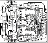
that were also no good.I'm attaching a shot of the artwork for which permission has been granted and which I described as a bit leggy earlier on. Its not great on resolution but should give a general impression hopefully.
What do you guys think?
Could parasitics be playing a part here because I to say that the original sim of the amp was fine as tested. I also looked at square-wave testing the original at HF and that was super clean as well.
Attachments
The problem with my resistor-inter-mid-point idea is that there is no phase reversal between the two points, through all those transistors on the way.Now trying 2k and again, it oscillates.
And since no phase reversal - no means of applying some local negative feedback.
The inter-midpoints resistor basically introduced positive feedback, if I am not mistaken. Which is actually shooting oneself in the foot, inviting oscillations.
Nice ones, looking at those sim images... Intriguing, that they are modulated by some yet other stuff, which could be a potential clue.
.... Hey! .... This is a circlotron, right? So there is a similar, mirrored set / branch of elements in parallel to the ones that I looked at on the upper side of the schematic.... Is this circlotron driven by a balanced, differential signal? If indeed, then I think I know how to make that local feedback thing "negative". ...
Please try to simulate the following two simultaneous connections: The first connection: Midpoint of resistors: R23--R30 (those in the upper branch) with the midpoint of resistors: R92--R93 (those in the lower branch), with a feedback resistor of some single kiloohms range. At the same time, make a second connection: Midpoint of resistors: R22--R60 (those in the lower branch) with the midpoint of resistors: R68--R69 (those in the upper branch), with a feedback resistor of exactly the same value as in the first connection.
The lower branch (I guess) is out-of-phase with the upper branch. So, this way, you will be essentially creating symmetrical negative feedback for those sections. Which may work, but probably could also not work, because this "cris-cross tilted 8" type of connection is has a fairly long route, and adds to the complexity of the loops within that are already there. Just fishing.
Does the amp oscillate in the same manner, when switched from SE input to balanced XLR inputs, driven by a set of two balanced input signals? Is there not something "fishy" about the input phase inverter on those two op-amps, with those ultra long criss-cross paths? Why not shorter paths, locally to those two op-amps (solely for the purpose of inverting, and not much else) ?
Instead of a "large criss-cross" loop, spanning a huge count of elements and surface area (look at those four 33 ohm resistors...), why not introduce two smaller loops, one alone just for the input inverter-opamps, and the other for the discreet silicon stuff ?
As in Julius Cesar: "Divide and rule (Latin: divide et impera), or divide and conquer, in politics and sociology is gaining and maintaining power by breaking up larger concentrations of power into pieces that individually have less power than the one implementing the strategy." {wiki}
There are two loooong wires, of global negative feedback, spanning from the almost-speaker-output-rail (the pre-inductor speaker rails), back to the input circuitry, to the resistors R42 and R109. This is ... very global.
Question: If you omit , within your simulation, just for the sake of a mental experiment, the output stage, and take/tap these two feedbacks paths from earlier points, such as: R10-R23 midpoint, and from R22-R60 midpoint (essentially "skipping out" on the output power stage and shortening the loop) - does that change anything in terms of stability? Does the such created "Front-End NFB" (omitting the output stage) still oscillate?
Would it be possible to introduce "ripple-eliminating" regulators for those parts of the supply rails, that feed the front end? Simple gyroscopes/capacitance multipliers (transistor with capacity at its base, and some voltage divider/time constant resistors to polarize the base)?
Is the midpoint of the speaker grounded? (4+4=8 ohms, midpoint grounded ...) Is there any "symmetrization resistors" that create a virtual ground for the midpoint of the speaker?
What is the "common reference" between the floating circlotron'ic batteries supplying the output stage, and the ground referenced front end? Where is it? Such common reference? I can't find it on the schematic. Please try adding the following circuit between the two speaker rails (before output inductors): 330R/5W + 330R/5W. (non-inductive). The midpoint of these - to the analog ground of the input stage. (Maybe it is there on the schematic somewhere, such or similar symmetrization, ... but I can't find it).
Why is there only one Q13 transistor, and not two? Should not each branch have its separate current drain?
Why is the current drain referenced to -43 Volts, and not to Ground ??
Is the midpoint of the speaker grounded? (4+4=8 ohms, midpoint grounded ...)
Is there any "symmetrization resistors" that create a virtual ground for the midpoint of the speaker? What is the "common reference" between the floating circlotron'ic batteries supplying the output stage, and the ground referenced front end? Where is it? Such common reference? I can't find it on the schematic.
Please try adding the following circuit between the two speaker rails (before output inductors):
330R/5W + 330R/5W. (non-inductive).
The midpoint of these - to the analog ground of the input stage.
(Maybe it is there on the schematic somewhere, such or similar symmetrization, ... but I can't find it).
Perhaps I can help a little. This is one channel only. It's a mono block. I am new to amplifier design and especially the concept of Circlotron. There is an excellent article on PassDiy that helped me a lot. Also this is a 'floating' bridge design. This is possible because being a mono block, the amplifier will never be operated unbridged. The speaker ground is a virtual ground as you have already established, and there is no shared wired ground connection with the 'front end' circuit and the Circlotron power supply. In simulation I replaced the 8 ohm load with 2 x 4 ohm resistors in series. Then I measured between this virtual ground and the driver board ground, they are virtually the same - pun intended
So, looking at the way the power supply is drawn, the driver board is fed from a transformer with a centre tap. The supplies for the Circlotron have no centre tap, just one winding pair for each bridge rectifier. I have been wondering what the benefits of a Circlotron design really are (the bridging part I get). Perhaps it keeps the large speaker return currents out of the driver circuits ground, seeing as they are effectively isolated?I'll have a read through all this slowly but I can answer a couple of points.
Why only one Q13... I don't know the design reasoning for this but yes, this indeed bias setting component is shared between the two halves.
I believe the amp oscillated irrespective of using balanced or single ended configurations.
Removing the output stage is something I looked at and tried... and yes its stable in that state but please don't lose sight of the fact that the simulation instability comes solely from my adding the parasitic inductance to the driver feeds. Without that inductance the sim is stable.
Adding active ripple filtering is probably not an option tbh, I say that because doing so takes it well outside the realm of a service tech working on these.
I'm also not sure how well the PSU setup reflects the actual real world amp. As drawn in the sim it is a standard split rail supply with audio referenced to the midpoint. The speaker does connect between the two halves as shown with the opamp servo's keeping the offset down. That's another oddity to me, the servo component values. 10uF caps and 33k resistors wrapped around the opamp rather than the more usual 1uF film cap and 1 to 10 meg resistor.
Fair enough .... Ziggy as "Advocatus diaboli": The base of Q1 is forward biased and controlled by the (ground referenced!) front end, andbiase d with a voltage .... referenced to WHAT ? ? ? The emiter of Q1 - what voltage does it have relative to the voltage of it's (ground referenced!) base? The "-43" volts rail would not be my best choice of a stable return / reference. The base of Q30 is forward biased and controlled by the (ground referenced!) front end, and biased with a voltage .... referenced to WHAT ? ? ? The emiter of Q30 - what voltage does it have relative to the voltage of it's (ground referenced!) base? What I am missing is a "return path" from the emitters of Q1 and/or Q30 back to the front-end-ground. Vbe ... is a voltage. Voltages are between two points, not one. If the base of the Vbe is polarized by the front end electronics, polarized "relative to front-end ground", it is my humble opinion that to complete the circuit, the emmiters of Q1 and Q30 need to "see" the ground of the front end, so that the Vbe can exist. Not to mention, that the 'reference' need be hum-free.Perhaps I can help a little. This is one channel only. It's a mono block. I am new to amplifier design and especially the concept of Circlotron. There is an excellent article on PassDiy that helped me a lot. Also this is a 'floating' bridge design. This is possible because being a mono block, the amplifier will never be operated unbridged. The speaker ground is a virtual ground as you have already established, and there is no shared wired ground connection with the 'front end' circuit and the Circlotron power supply. In simulation I replaced the 8 ohm load with 2 x 4 ohm resistors in series. Then I measured between this virtual ground and the driver board ground, they are virtually the same - pun intended
My suggestion with two 330R/5W resistors from each of the pre-coil speaker rails to ground, as a means of "symmetrization" - still holds.
Would it be possible to try it on a REAL amp ?
Even in the most basic wiki definition of the circlotron: Circlotron - Wikipedia There is a picture that shows the concept of symmetrization: Circlotron - Wikipedia Without the two equal valued resistors, the device will not work properly. This is because each of the gates / bases / grids of the active devices needs to "see" the reference. The output stage has indeed floating batteries, but the device that controls the gates/bases/grids - is ground referenced. Hence the need for the resistors. These create a "virtual ground", i.e. a "mid-point" within the speaker. "Something" that you can "reference to".
It could be argued, that within a circlotron, you do not need to use complementary devices within the output stage. You do not have to mix PNP with NPN, as in a classical architecture with symmetrical rails (+, -) and ground in the center. In the circlotron, you use two devices of same characteristics: NPN + NPN.I have been wondering what the benefits of a Circlotron design really are
Easier to pair, same behavior. But fret not, the circlotron also has some major drawbacks. Peak-to-Peak output swing, for example.
Why is there only one Q13 transistor, and not two?
Should not each branch have its separate current drain?
Why is the current drain referenced to -43 Volts, and not to Ground ??
In the simulation, the collector of Q13 sits at approx -7.5v. The junction of R20 and R28 sits at a slightly negative voltage with respect to ground. So this peculiar bias arrangement seems to work by making Q1 emitter more negative with respect to the base, rather than the usual vbe multiplier that would normally drive the base higher, if that makes any sense. I've never seen anything quite like this before. Has anyone else? I'd love a link if you have.
The annoying little ??? in the PDF should be voltages. This happens when the PDF is printed before the sim is run. Perhaps Mr Mooly would be kind enough to provide us with a new one with voltages?
Pretty please?It could be argued, that within a circlotron, you do not need to use complementary devices within the output stage. You do not have to mix PNP with NPN, as in a classical architecture with symmetrical rails (+, -) and ground in the center. In the circlotron, you use two devices of same characteristics: NPN + NPN.
Easier to pair, same behavior. But fret not, the circlotron also has some major drawbacks. Peak-to-Peak output swing, for example.
Yes, excellent point, I had forgotten about that. This output stage is all NPN, also known as quasi complementary I think. I have seen those before but in non-Circlotron form so when working from a single supply the midpoint is half the supply voltage and you need an output capacitor.
What do you mean by peak to peak output swing limitations? Can you tell me more?
..........The annoying little ??? in the PDF should be voltages. This happens when the PDF is printed before the sim is run. Perhaps Mr Mooly would be kind enough to provide us with a new one with voltages?
I shall ask
as I can't seem to produce a PDF myself with anything like the fine resolution of the one that was sent to me earlier... unless there is some secret to doing it.- Home
- Amplifiers
- Solid State
- CFA Class A Circlotron with stability issues. Thoughts invited.