Next Problem with faulty rubish SONY VFET Design:
The symmetry adjust does of the power amplifier does not correct with
real load.
This happens because the conduction resistors
(Ron) of the MOSFETs N and P are not equal. Channel P has
a higher Ron than channel N. This characteristic depends on
the MOSFET's physical construction.
The threshold voltage varies much, even between
MOSFETs of the same kind. When connecting them in
parallel we must be careful that they all have the same
conduction current if we want equal currents circulating in all
of them.
If the conduction voltage of P an N channels
MOSFETs is not the same they will conduct different
currents, even when we apply identical gate-source voltages.
As the bias current of the N MOSFETs must be identical to
the one of the P MOSFETs the feedback will correct the
continuous voltage at the operational output to polarize the
MOSFETs with different voltages until both conduct equal
currents.
To avoid this we must put a symmetry adjust in VFET amp
Only N Channel output devices Amp no need symmetry adjust
Afer many amps blow up in the 70s, Sony stop VFET forever
Reason why the V-FET's are special had been explained in Pass site on V-FET designs/ articles. if one is patient, the amp can be brought back to life. One has to listen to a working amp to understand why there are many followers to these Amps. before restoring read as many postings on Audio Karma website - has more posting on them than this one. I have both Yamaha and Sony V-FET amps and restored TA 5650. I can confidently say it is worth restoring
kannan
kannan
VFET are great sounding amps, but discontinued from Sony and Yamaha late 70s
Poor rubbish circuit design:
1. Sony used an varactor dual-diode package in the bias circuitry of these amps, often they fail and kill the VFETs -
Sony Vfet = self destructing amp
2. Audio circuit is not reliable, engineering faults, a lot of service bulletin updates
3. To much heat for small power decrease lifetime for VFET devices
VFETs have an internal resistance 4 times greater than Bipolar Transistors or 7 times greater than switching mosfets.
This means a lot of heat compare to BJT devices already in standby,
4. Mosfet amp with IRFP / IXYS switching mosfets are cold at same Voltage/Output power
same great sound experience without any problems like old poor 70s Sony design
Reason why the V-FET's are special had been explained in Pass site on V-FET designs/ articles
I can confidently say it is worth restoring
kannan
I want try to buy 2 N Channel VFETs and put in my design
If somebody have not matching from same grade P/N parts available
I want buy the N Channel only and try
There are many VFET offer in Ebay for abou 70 EUR/USD , can I trust and buy ?
I am sure you could have done a better job if you were in those Sony engineers’ shoes back in 1970s, NMOS. But, coming back to the original question of mine, do you have a non-destructive method to characterize and match the V-Fets?
Next Problem with faulty rubish SONY VFET Design:
The symmetry adjust does of the power amplifier does not correct with
real load.
This happens because the conduction resistors
(Ron) of the MOSFETs N and P are not equal. Channel P has
a higher Ron than channel N. This characteristic depends on
the MOSFET's physical construction.
The threshold voltage varies much, even between
MOSFETs of the same kind. When connecting them in
parallel we must be careful that they all have the same
conduction current if we want equal currents circulating in all
of them.
If the conduction voltage of P an N channels
MOSFETs is not the same they will conduct different
currents, even when we apply identical gate-source voltages.
As the bias current of the N MOSFETs must be identical to
the one of the P MOSFETs the feedback will correct the
continuous voltage at the operational output to polarize the
MOSFETs with different voltages until both conduct equal
currents.
To avoid this we must put a symmetry adjust in VFET amp
Only N Channel output devices Amp no need symmetry adjust
Afer many amps blow up in the 70s, Sony stop VFET forever
I am sure you could have done a better job if you were in those Sony engineers’ shoes back in 1970s, NMOS. But, coming back to the original question of mine, do you have a non-destructive method to characterize and match the V-Fets?
>only the 2SJ18s seems to be shorted (2 from each channel) and the rest has >the same Vgs value as they are factory matched, I think.)
Sorry cant help you
The amp can work with 2 pair each channel too, no problem
take out the N channel, who no habe P channel and problem is solved
VFET are great sounding amps, but discontinued from Sony and Yamaha late 70s
Poor rubbish circuit design:
1. Sony used an varactor dual-diode package in the bias circuitry of these amps, often they fail and kill the VFETs -
Sony Vfet = self destructing amp
..As did about 50 other manufacturers and all had the same problems with them. This has nothing to do with circuit design, rather with component selection - which were later proven to be unreliable. So have many other early plastic cased devices in many manufacturers devices.
2. Audio circuit is not reliable, engineering faults, a lot of service bulletin updates
I am aware of only one actual update, and that was for the smaller integrateds. None of them had to do with VFETs.
3. To much heat for small power decrease lifetime for VFET devices
Typical VFET ide currents are 100mA per output pair, same or lower than older and contemporary MOSFET designs. Depending on actual amp, power output is lower as this is limited by RDSon
VFETs have an internal resistance 4 times greater than Bipolar Transistors or 7 times greater than switching mosfets.
This means a lot of heat compare to BJT devices already in standby,
I would recommend a LOT of reading before posting something as incorrect as this. Power disspation is current times voltgage over a device. For the same power supply and idle current, every device will generate the same heat. THis has nothing to do with internal resistance and internal resitance has nothing to do with heat at standby. The ide current is set up to get the best linearity out of the output stage and with VFETs it is about as good as you can get - provided the proper idle conditions are set. Also, VFETs don't strictly have a crossover region when implemented as a complementary output stage, but that's a whole different post.
Also, VFETs can be driven into very low RDSon mode, and indeed were in the original switching circuits they were intended for (yes, the first use was NOT audio). In that regard they still offer fastest switching speeds of all semiconductor architectures, which is now coming back with SiC semiconductors.
4. Mosfet amp with IRFP / IXYS switching mosfets are cold at same Voltage/Output power
Nothing is cold at the same output power unless it's a class D amp. VFETs do have a higher idle current and higher losses (depending on circuit they can be a lot higher, and here I am limiting myself to linear curcuits). This is a scarifice made to maintain maximum linearity.
same great sound experience without any problems like old poor 70s Sony design
Good luck with that...
To much Sony VFET amps not working reliable and blow up, there was no future for VFETS and Sony stop late 70s production.
Not for reasons of unreliability. VFETs are actually quite robust, But if your fuses blow and you insist on replacing them with ever greater values 10 times in a row, something else will die, and it's usually the component that handles most of the power, that being a VFET.
Reason VFETs were discontiued was they were >10x more expensive to make than any other semiconductor.
Same with lateral Audio Mosfets in Professional PA amplifier.
Actually, cheaper laterals were the reason for VFET's demise. By the time Hitachi made them, FET was already an established acronym for 'good sound', so they capitalized on it. Let me just say that Hitachi also made VFETs. At the time they invested heavily into NMOS/CMOS process used to second source many memory and microprocessor components from USA suppliers, which made it possible for them to cheaply manufacture audio lateral MOSFETs and severely undercut VFET prices.
Many years ago Amplifier manufacturer stop Production with audio Mosfets about similar problems like VFETS
Really? I actually work in the PA amplifier business and I am asked about availability of lateral MOSFETs almost on a daily basis. They are still made, slightly better process control on the very same dies. Even Renesas (ex Hitachi semi) obsoleted the oldest one (J162/K1058) relatively recently.
IF you manage to find them any more. The old IRFP line that was fully characterized for linear performance has long been on the way out. Today's faster replacements can be very problematic re SOA when used in the linear mode.With Switching mosfets you can build very rugged reliable Class AB amplifier
Next Problem with faulty rubish SONY VFET Design:
The symmetry adjust does of the power amplifier does not correct with
real load.
Completely wrong. Unlike MOSFETs, the channel conduction of VFETs is overwhelmingly dependant on the channel design, which is what results (indirectly) in triode-like curves, unlike any other semiconductor. As a result, although manufacturing tolerances are large, P and N parts can be well optimized to be complementary, and in fact Sony units are optimized for that (but eg. NEC and Yamaha are not). They also have a MUCH lower gate capacitance compared to even similar MOSFETs.
It is difficult to find original info on Sony VFETs but even what there is is very limited. However, I have personally traced literally hundreds of VFETs on a Tek tracer, and when the rank is the same, they are remarkably complementary, more so than even lateral MOSFETs, where they bent over backwards to make them so (resulting in completely different silicon dies for the N and P part).
If proper rank VFETs are used in the Sony amps, there is no problem with symmetry. In fact, there is an AES paper ot there describing an output stage with said VFETs, IIRC it has less than 0.3% distortion without any form of NFB. That is outstanding for any sort of FET output.
This happens because the conduction resistors
(Ron) of the MOSFETs N and P are not equal. Channel P has
a higher Ron than channel N. This characteristic depends on
the MOSFET's physical construction.
VFET is not MOSFET.
The threshold voltage varies much, even between
MOSFETs of the same kind. When connecting them in
parallel we must be careful that they all have the same
conduction current if we want equal currents circulating in all
of them.
...VFET is not MOSFET.
If the conduction voltage of P an N channels
MOSFETs is not the same they will conduct different
currents, even when we apply identical gate-source voltages.
As the bias current of the N MOSFETs must be identical to
the one of the P MOSFETs the feedback will correct the
continuous voltage at the operational output to polarize the
MOSFETs with different voltages until both conduct equal
currents.
... ... VFET is not MOSFET.
To avoid this we must put a symmetry adjust in VFET amp
Only N Channel output devices Amp no need symmetry adjust
This is really amusing since there is no reason why only P-ch amps would need such adlust also being 'same sex' output. But the really amusing part is, the Yamaha B1, being THE quintessential VFET amp, uses only N ch outputs and it's the only one that actually has a symmetry adjustment
")
Yamaha did develop a complement to the B1's 2SK77 output VFET (a huge 300V 20A device), the 2SJ27, but they never used it because these were only used in the B1 which was an extremely expensive very low production number amp, so selecting ranks of both P and N type VFETs with probably half of the production ending up not being used was dropped in favor of a N-ch totem pole output.
Sony used a different path, optimizing their VFETs for complementarity, rather that maximum transconductance and minimum RDSon.
That being said, VFETs have a positive gate current region where they exhibit a sort of Beta like bipolars, but without secondary breakdown. In tihis mode RDSon is reduced easily by a factor of ten even for only a few mA of gate current. This was used in one of the first class D designs, the Sony TA-N88. There, two pairs of VFETs (in a discrete circuit!) switch at 500kHz rates with transition times of ~80ns from one to the other 80V rail. That was in 1978. Even today doing this with modern fast MOSFETs requires a lot of effort.
Last edited:
To original author of the thread:
1) Be aware WORKING VFETs will measure near short S-D (actually Rdson at Vgs=0 since these are depletion devices, i.e. they are normally on and control voltage turns them off).
2) Do not trust markings on devices you can buy on ebay etc. These are most likely genuine devices but they recycle them and re-mark them, while having no idea the rank number actually means something. I've had batches of VFETs all marked rank 57 actually be all sorts of ranks, and sometimes even not the right type of VFET (J28 instead of 18, K82 instead of K60, and the other way around). Sometimes they are also remarked NEC and Yamaha VFETs and some times they are also remarked BJT blown to short C and E 'emulating' a VFET.
3) It is necessary to use same rank VFETs in these amps. They will work for test purposes and low loads with one less pair but this should not be permanent. In fact, when testing intially it is common practice to only install one pair (and adlust a much lower - 1/4 - idle current).
4) There is a way to test the rank using two power supplies with some current limiting. The 8550 service manual actually gives you Vgs values to expect at the rated idle current and Vds (Vds being one supply rail). This can be simulated on a bench, but the VFET must be on a heatsink as it will be placed into real idle state conditions.
5) IF mixed ranks of VFETs must be used because of availability, then the ranks should differ at most 1, and all J types must be the same rank, also K types the same rank. For example, if all Js are rank 56, then Ks must all be either 55,56, or 57. However, this arrangemet gives higher (even harmonic) distortion and potentially uneven clipping. Also, higher ranks will produce a bit more power as their Rdson is lower.
6) unlike smaller amps, it's not dead easy to start up the amp without VFETs at all in order to verify circuit functions before installing the VFETs but it can be done - I will leave it to another post.
7) DO NOT start the amp on a variac. Actually the 5550 and 8550 have a higher chance of surviving this but it is NOT recommended. The reason being, the circuit relies on the bias supply (front end supply) coming up quicker than the main output power in order to prevent cross-conduction. If a variac is used, this can happen and last long enough to blow the output stage, though it is unlikely with the right rating fuses. Unfortunately, people tend to replace blown fuses with larger ratings and... well, not difficult to tell where this leads. The method of starting the amp with no VFETs mentioned in (6) can safely be used without a variac.
First Lesson Learned!
After ilimzn mentioning about a Service Bulletin regarding the measurements of the VFETs, I've made a quick search to find it. I dusted off my reliable Triplett Model 630-PL and set it to x1 in the ohms scale.
I started following the bulletin and run the following measurements
1- S to D should read approximately 1 to 2 ohms.
2- S to G should read like a diode
3- D to G should read like a diode
The above 3 points were all okay for the VFETs that PEAK equipment deemed bad! Was it a struck of luck that the VFETs fixed themselves in between the time I last measured them?
My hopes of VFETs fixing themselves was short lived, as I started to measure and note down the S-D resistances of all the 12 VFETs came out of the amplifier. It is now clear to me that the PEAK equipment has a threshold resistance value for judging shorts. All the VFETs it deemed bad had below 1.5ohm S-D reading and all the ones it gave a green check mark had above 1.5ohm reading with the Triplett.
Moral of the story, PEAK DCA75 Pro may deceive you and make you throw away your valuable, working VFETs to the trash if you don't know what you are doing.
So, I think I ended up having 12 healthy VFETs after all. Correct knowledge is more valuable than gold these days All thanks to ilimzn!
/Dirk
After ilimzn mentioning about a Service Bulletin regarding the measurements of the VFETs, I've made a quick search to find it. I dusted off my reliable Triplett Model 630-PL and set it to x1 in the ohms scale.
I started following the bulletin and run the following measurements
1- S to D should read approximately 1 to 2 ohms.
2- S to G should read like a diode
3- D to G should read like a diode
The above 3 points were all okay for the VFETs that PEAK equipment deemed bad! Was it a struck of luck that the VFETs fixed themselves in between the time I last measured them?
My hopes of VFETs fixing themselves was short lived, as I started to measure and note down the S-D resistances of all the 12 VFETs came out of the amplifier. It is now clear to me that the PEAK equipment has a threshold resistance value for judging shorts. All the VFETs it deemed bad had below 1.5ohm S-D reading and all the ones it gave a green check mark had above 1.5ohm reading with the Triplett.
Moral of the story, PEAK DCA75 Pro may deceive you and make you throw away your valuable, working VFETs to the trash if you don't know what you are doing.
So, I think I ended up having 12 healthy VFETs after all. Correct knowledge is more valuable than gold these days
All thanks to ilimzn!/Dirk
Normal equipment with automatic measuring has no notion of VFETs so it will not recognize them correctly. VFETs are so rare in the entire history of semiconductors that this is not so surprising, but as you said, before using such equipment one has to know the basics of what is measured or some real problems can arise - 6 pairs of VFET are worth at least 600EUR _IF_ you can even find them.
Now, it is very likely you have a set of working ones in your amplifier, but apart from measuring on a curve tracer, almost impossible to know if they are up to full spec. Fortunately (and contrary to popular opinion) VFETs are actually rather sturdy and over specified (Vdsmax 160V VFETs regularly withstand 200-250V).
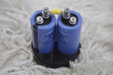
That being said, make sure to rebuild and fix everything else there is to fix in the amplifier. Unfortunately one point of trouble is the dual main filter cap. These have been problematic in almost every amplifier I have seen them in. They tend to internally corrode the middle contact, resulting in a 'floating' power supply. They can usually be replaced by 4 smaller ones that will take the same space in a 2x2 array, connected externally to form the right capacitance and center point connection. It takes some work to fix them mechanically instead of the one dual capacitor.
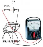
Finally, VFETs can be tested to some degree by using a 9V block battery with a series resistor (anything 470 ohms to a few k ohms will do) to limit gate current in case you connect it wrong.
To test, you can connect an ohm-meter between S and D to measure resistance. Polarity of the connection is important, as I will outline below.
The 9V battery connected through the series resistor is then used to polarize the gate so the VFET turns off. Since ohm-meters only supply a small voltage or current to test resistance, the 9V bias from the battery should be able to turn the VFET off completely (the resistance will show a much higher value, 10s to 100s of k and sometimes even completely open circuit).
The connection is as follows:
For N ch VFET (2SK60) connect positive lead of the ohm meter to D (case), negative to S. Verify that it shows the usual 1-2 ohms. Then connect the battery positive to S and negative to G. This will apply a 9V negative bias. Now the ohm-meter should show practically open circuit.
For P ch VFET (2SJ18) connect negative lead of the ohm meter to D (case), positive lead to S. Again, verify that it shows the usual 1-2 ohms. Then connect the battery negative to S, positive to G. This applies a 9V positive bias (but for the P-ch part) so the VFET should turn off and show practically open circuit.
Warning: some analog instruments (with pointer movement) use reverse polarity when set to measure resistance. You can verify the correct polarity measuring G-S or G-D which should show a diode.
This measurement is sometimes also possible with two digital multimeters, set to diode test. Again, one goes D-S, the other S-G. The red lead is normally diode anode (positive) the black lead diode cathode (negative). The multimeter applies a current limited voltage of around 1.5 to 3V depending on make and model. This is already enough to check that the VFET behaves properly but the change in conductivity D-S will not be as pronounced. However, since the tester is current limited, you can also test G-S in the positive biassed mode, when it shows a conducting diode. When you do that, the multimeter set to monitor D-S conductivity will show REDUCED resistance, often to a point indistinguishable from a short circuit.
Now, it is very likely you have a set of working ones in your amplifier, but apart from measuring on a curve tracer, almost impossible to know if they are up to full spec. Fortunately (and contrary to popular opinion) VFETs are actually rather sturdy and over specified (Vdsmax 160V VFETs regularly withstand 200-250V).
That being said, make sure to rebuild and fix everything else there is to fix in the amplifier. Unfortunately one point of trouble is the dual main filter cap. These have been problematic in almost every amplifier I have seen them in. They tend to internally corrode the middle contact, resulting in a 'floating' power supply. They can usually be replaced by 4 smaller ones that will take the same space in a 2x2 array, connected externally to form the right capacitance and center point connection. It takes some work to fix them mechanically instead of the one dual capacitor.
Finally, VFETs can be tested to some degree by using a 9V block battery with a series resistor (anything 470 ohms to a few k ohms will do) to limit gate current in case you connect it wrong.
To test, you can connect an ohm-meter between S and D to measure resistance. Polarity of the connection is important, as I will outline below.
The 9V battery connected through the series resistor is then used to polarize the gate so the VFET turns off. Since ohm-meters only supply a small voltage or current to test resistance, the 9V bias from the battery should be able to turn the VFET off completely (the resistance will show a much higher value, 10s to 100s of k and sometimes even completely open circuit).
The connection is as follows:
For N ch VFET (2SK60) connect positive lead of the ohm meter to D (case), negative to S. Verify that it shows the usual 1-2 ohms. Then connect the battery positive to S and negative to G. This will apply a 9V negative bias. Now the ohm-meter should show practically open circuit.
For P ch VFET (2SJ18) connect negative lead of the ohm meter to D (case), positive lead to S. Again, verify that it shows the usual 1-2 ohms. Then connect the battery negative to S, positive to G. This applies a 9V positive bias (but for the P-ch part) so the VFET should turn off and show practically open circuit.
Warning: some analog instruments (with pointer movement) use reverse polarity when set to measure resistance. You can verify the correct polarity measuring G-S or G-D which should show a diode.
This measurement is sometimes also possible with two digital multimeters, set to diode test. Again, one goes D-S, the other S-G. The red lead is normally diode anode (positive) the black lead diode cathode (negative). The multimeter applies a current limited voltage of around 1.5 to 3V depending on make and model. This is already enough to check that the VFET behaves properly but the change in conductivity D-S will not be as pronounced. However, since the tester is current limited, you can also test G-S in the positive biassed mode, when it shows a conducting diode. When you do that, the multimeter set to monitor D-S conductivity will show REDUCED resistance, often to a point indistinguishable from a short circuit.
That being said, make sure to rebuild and fix everything else there is to fix in the amplifier.
The following is from a similar TAN-8550 restoration thread on AK:
I am also replacing critical components for the bias supply side of both boards. This includes bias Resistors R725/775 and R731/732 and R781/782.
Also the 220K trim pots RT 701and 751 will come out. I will set these to the same value as the pulls before I install them. Also changing out Q713-716 and Q763-766, as the service manual states that failure of these transistors will cause V-FET failure.
I can follow the requirement for the change of the 220K trim pots, as these were a major source of problems in my Revox A77 restoration. Although all the other components were good, the intermittent connection in such pots ruined almost everything. I am also going to check the resistors and see if they are still in tolerance, however, is replacing the transistors mentioned above too much or do you think that it is a necessary precaution as they can drift or become noisy over time?
Unfortunately one point of trouble is the dual main filter cap. These have been problematic in almost every amplifier I have seen them in. They tend to internally corrode the middle contact, resulting in a 'floating' power supply. They can usually be replaced by 4 smaller ones that will take the same space in a 2x2 array, connected externally to form the right capacitance and center point connection. It takes some work to fix them mechanically instead of the one dual capacitor.
I have already ordered 2x 10000uF 100V capacitors that are 35mm in diameter and 100mm tall. I have seen a similar approach from an AK member and looked like a clean solution to me. I was hesitant to replace this capacitor, though. As I was following the common belief that "the larger the capacitor, the lower is the chance that it would go bad". But, now that you are also mentioning a possible problem with it, I will definitely attend to it and replace it with the two new ones.
Finally, VFETs can be tested to some degree by using a 9V block battery with a series resistor (anything 470 ohms to a few k ohms will do) to limit gate current in case you connect it wrong.
To test, you can connect an ohm-meter between S and D to measure resistance. Polarity of the connection is important, as I will outline below.
The 9V battery connected through the series resistor is then used to polarize the gate so the VFET turns off. Since ohm-meters only supply a small voltage or current to test resistance, the 9V bias from the battery should be able to turn the VFET off completely (the resistance will show a much higher value, 10s to 100s of k and sometimes even completely open circuit).
The connection is as follows:
For N ch VFET (2SK60) connect positive lead of the ohm meter to D (case), negative to S. Verify that it shows the usual 1-2 ohms. Then connect the battery positive to S and negative to G. This will apply a 9V negative bias. Now the ohm-meter should show practically open circuit.
For P ch VFET (2SJ18) connect negative lead of the ohm meter to D (case), positive lead to S. Again, verify that it shows the usual 1-2 ohms. Then connect the battery negative to S, positive to G. This applies a 9V positive bias (but for the P-ch part) so the VFET should turn off and show practically open circuit.
Warning: some analog instruments (with pointer movement) use reverse polarity when set to measure resistance. You can verify the correct polarity measuring G-S or G-D which should show a diode.
This measurement is sometimes also possible with two digital multimeters, set to diode test. Again, one goes D-S, the other S-G. The red lead is normally diode anode (positive) the black lead diode cathode (negative). The multimeter applies a current limited voltage of around 1.5 to 3V depending on make and model. This is already enough to check that the VFET behaves properly but the change in conductivity D-S will not be as pronounced. However, since the tester is current limited, you can also test G-S in the positive biassed mode, when it shows a conducting diode. When you do that, the multimeter set to monitor D-S conductivity will show REDUCED resistance, often to a point indistinguishable from a short circuit.
To demonstrate that I understood the layout correctly, I prepared a basic diagram and attached it below.
Attachments
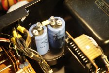
The dual capacitors have been a problem in many amps, including both TAN8550 and TA8650, several Hitachi amps, and most notably Yamaha B1 which will result in VFET failure (and those are REALLY hard to find).
At the moment I can't look up the schematic to see about the transistors, but it is possible, some of the ones in several Sony amps of the time are among the ones that tend to fail due to early plastic encapsulation suffering from moisture ingress, ultimately oxidizing the internal contacts to the semiconductor die, also resulting in damage to the semiconductor and leaky or breakdown prone transistors. The good question is what to replace them with... were there any suggestions given?
PS - the diagram is correct!
At the moment I can't look up the schematic to see about the transistors, but it is possible, some of the ones in several Sony amps of the time are among the ones that tend to fail due to early plastic encapsulation suffering from moisture ingress, ultimately oxidizing the internal contacts to the semiconductor die, also resulting in damage to the semiconductor and leaky or breakdown prone transistors. The good question is what to replace them with... were there any suggestions given?
In that case, those transistors were replaced by the NOS components. I would still suspect that the moisture ingress should work the same way for the NOS components as much as the components in the field, so it does not guarantee a healthy replacement. It can be difficult to find a perfect replacement, as I see some additional markings (red pen marks) over the transistors as if they have gone through a secondary matching process.
As for the VFETs, I have prepared the circuit and checked all all the VFETs. One thing that I noticed worried me. When I am checking the 2SJ18s that PEAK said they were good, the recovery time going from an almost open circuit state to 1-2ohm takes about 9-10seconds, but the ones that are said to be bad, it takes shorter time like 1-2seconds. Besides, the ones that take a long time to recover, it is enough for me just to touch the G terminal for a very short amount of time with the battery terminal to open the circuit, the other ones however, I need to hold the connection till the meter reaches to the open circuit condition. Does this mean anything?
Last edited:
Heating can easily cause an irreversible change in the silicon dioxide layer. Rather, the problem lies in the reckless circuit designs and overloading. If the signal power produced with soundly judged device capabilities is insufficient, maybe it is better to stick to more rugged commonplace transistors.
To my thinking extreme heating caused by reckless circuit designs can easily do irreversible damage to the silicon layers. But as Ilimzn has already explained in generous and knowledgeable detail, there was nothing reckless about both V-FET and V-FET circuit designs back then with Yamaha, Sony and a few others. Sadly, BJT's and MOSFET's were much cheaper to manufacture and as such, these days amps using these sonic beauties are now avoided for their V-FET rarity.Heating can easily cause an irreversible change in the silicon dioxide layer. Rather, the problem lies in the reckless circuit designs and overloading. If the signal power produced with soundly judged device capabilities is insufficient, maybe it is better to stick to more rugged commonplace transistors.
Last edited:
Let me explain what I meant in a bit more detail.
This does not have to do with improper use of the semiconductors and exposing them to stress outside the specified maximums, nor the specifications being over-estimated. In fact, if anything, VFET specifications are underestimated.
What i am talking about are other components used regularly in amplifiers of the time, and by many manufacturers.
In particular, early plastic encapsulated parts would fail 20-30 years on in various ways. One of the typical ones is moisture (and indeed other contaminants) entering the case through a failing metal to plastic interface. For instance, some then common small signal BJTs made by Hitachi and other second sources were extremely prone to this - the pins would corrode and the corrosion would slowly proceed towards the inside of the plastic case, eventually resulting in the interface not sealing any more at which point various contaminants could enter (one of the leading ones being from tobacco tar!). Other components, like the already mentioned multi-diodes (also known as 'bead diodes' because of the way the case looks, like small plastic beads with thin wires coming out of oposite sides), which would go open circuit. Since they were used as voltage references for current sources or thermal compensation in bias circuits in most cases, when they go open, the result is 'infinite current' and 'infinite bias', which would as a rule lead to serious failures within milliseconds. Some more failure-prone components became popular later on, in the late 80s and early 90s, there were the 'black flag' silver mica capacitors, who got their name because they look like small black epoxy-dipped rectangles, but also because they would spontaneously go open circuit and leave your amplifier without frequency compensation, turning it into an oscillator, which would then fry the output stage due to cross-conduction. Experienced vintage equipment restorers will replace all of these if they see them, not bothering to test if they still work - they are a hazard to other components which may have become unobtainable, and of course, no-one wants their amp, new or old, to fail 'inexplicably'.
That being said, let me also stress that none of the amplifiers talked about in this thread are 'perfect', as indeed, no amplifier is. Real world constraints, not the least of which are costs, have to be contended with in real world products.
For instance, in smaller VFET amplifiers from Sony, there is a mechanism that cold lead to cascade failures ending with VFETs when the power supply caps eventually go well below spec - let's not forget these amps are now ~40 years old and actually not designed to last that long (Though arguments could be made that a lot of clever engineering has gone into getting the most out of the parts available). There are posts here and on Audiokarma where a few simple fixes to this have been proposed and implemented. That being said, companies do learn if they want to stay in business - second generation VFET amps from Sony (and the rare one from Yamaha) worked around these issues by using different circuits. Again, keep in mind these are also over 30 years old and there are perishable components, notably electrolytic caps, so just like anything, these can't be expected to last forever without a good restoration job.
Last edited:
In that case, those transistors were replaced by the NOS components. I would still suspect that the moisture ingress should work the same way for the NOS components as much as the components in the field, so it does not guarantee a healthy replacement. It can be difficult to find a perfect replacement, as I see some additional markings (red pen marks) over the transistors as if they have gone through a secondary matching process.
You would be right on the potential unreliability of NOS components, which is why in most cases I try to find modern equivalents for older type semiconductors. They will eventually go bad for the same reasons even sitting in a box, and sometimes even quicker because they may have been stored in who knows what conditions for all these years.
It is also the case that some components which were 'leading edge' could have been selected when run close to maximum limits in a given circuit. This was done by many manufacturers, for simple reason: that was all that there was to chose from.
As for the VFETs, I have prepared the circuit and checked all all the VFETs. One thing that I noticed worried me. When I am checking the 2SJ18s that PEAK said they were good, the recovery time going from an almost open circuit state to 1-2ohm takes about 9-10seconds, but the ones that are said to be bad, it takes shorter time like 1-2seconds. Besides, the ones that take a long time to recover, it is enough for me just to touch the G terminal for a very short amount of time with the battery terminal to open the circuit, the other ones however, I need to hold the connection till the meter reaches to the open circuit condition. Does this mean anything?
Hm, when you apply the battery and the VFET goes 'open circuit', the G to (S+D) structure is a reverse biassed diode of a fairly large internal capacitance, and it can often be observed to discharge slowly, which is why it takes some time to go back to the fully conducting state. Discharging it from G to S by making a bridge with your finger or indeed a short circuit should restore full conduction (1-2 ohms) immediately.
The opposite should be the case when touching the battery to go to the non-conductive state, this should happen immediately. The 470 ohm series resistor is very small compared to the capacitances involved and the gate should charge up from the battery in less than a microsecond. However, you are measuring with very small S-D voltage and this actually increases the apparent capacitance but even if it is an order of magnitude more, it should be near immediate. When you measure G-S and G-D as diodes, what resistances does your multimeter show?
It should be noted that VFET gate to channel (Source-Drain structure) leakage current can be fairly high (100 uA is not uncommon) but very variable from VFET to VFET. The parts were never selected for this as it's not too relevant given the gate drivers should be low impedance and this slight current makes no difference in their operation. This might be producing the odd behavior.
Unfortunately, there is also the possibility that the VFETs are damaged. One of the most common failure modes for VFETs is blowing the external to internal gate terminal connection, by producing forward current into the gate. The current limit is quite high (500mA if I recall correctly) but when driver circuits fail, it's possible to produce even higher currents. This results in the internal wire bond acting as a fuse and burning out, resulting in a dead VFET. However, it's also possible to make this wire bond so hot due to excessive current that it will damage the VFETs semiconductor structure and degrade parameters. This is the second most common mode of failure, you are left with something that measures as a VFET but with degraded characteristics, sometimes severely so. Contrary to opinions, VFETs are hard to kill - unlike other semis, they don't simply go open or short, they degrade and 'fade'. Unfortunately, it is often possible to produce failure conditions for a LOT longer than in regular BJT or MOSFET designs, and this is the leading cause of VFET amp death - when fuses blow, it means something is wrong, not 'replace fuse with progressively thicker wire' until just about everything is wrong.
Unfortunately, the only way to know for sure if the VFETs are still OK (even this is more likely than with almost any other type of semiconductor), is to test them with a curve tracer :/
Do you know what the original failure of the amplifier was? You did mention the bead diodes being open...
V FETish,
any mode that wreaks damage and destruction is morally objectionable. The heating need not be extreme. The thick uncontaminated silicon dioxide layer used in the peculiar gate-source structure has a high negative temperature coefficient. Make sure that the V-FETs run cool by drastically reducing the rail voltages, increasing the size of the heat sink and moderating your listening practices. It will drastically reduce distortion as well.
any mode that wreaks damage and destruction is morally objectionable. The heating need not be extreme. The thick uncontaminated silicon dioxide layer used in the peculiar gate-source structure has a high negative temperature coefficient. Make sure that the V-FETs run cool by drastically reducing the rail voltages, increasing the size of the heat sink and moderating your listening practices. It will drastically reduce distortion as well.
Hm, when you apply the battery and the VFET goes 'open circuit', the G to (S+D) structure is a reverse biassed diode of a fairly large internal capacitance, and it can often be observed to discharge slowly, which is why it takes some time to go back to the fully conducting state. Discharging it from G to S by making a bridge with your finger or indeed a short circuit should restore full conduction (1-2 ohms) immediately.
The opposite should be the case when touching the battery to go to the non-conductive state, this should happen immediately. The 470 ohm series resistor is very small compared to the capacitances involved and the gate should charge up from the battery in less than a microsecond. However, you are measuring with very small S-D voltage and this actually increases the apparent capacitance but even if it is an order of magnitude more, it should be near immediate. When you measure G-S and G-D as diodes, what resistances does your multimeter show?
It should be noted that VFET gate to channel (Source-Drain structure) leakage current can be fairly high (100 uA is not uncommon) but very variable from VFET to VFET. The parts were never selected for this as it's not too relevant given the gate drivers should be low impedance and this slight current makes no difference in their operation. This might be producing the odd behavior.
Unfortunately, there is also the possibility that the VFETs are damaged. One of the most common failure modes for VFETs is blowing the external to internal gate terminal connection, by producing forward current into the gate. The current limit is quite high (500mA if I recall correctly) but when driver circuits fail, it's possible to produce even higher currents. This results in the internal wire bond acting as a fuse and burning out, resulting in a dead VFET. However, it's also possible to make this wire bond so hot due to excessive current that it will damage the VFETs semiconductor structure and degrade parameters. This is the second most common mode of failure, you are left with something that measures as a VFET but with degraded characteristics, sometimes severely so. Contrary to opinions, VFETs are hard to kill - unlike other semis, they don't simply go open or short, they degrade and 'fade'. Unfortunately, it is often possible to produce failure conditions for a LOT longer than in regular BJT or MOSFET designs, and this is the leading cause of VFET amp death - when fuses blow, it means something is wrong, not 'replace fuse with progressively thicker wire' until just about everything is wrong.
Unfortunately, the only way to know for sure if the VFETs are still OK (even this is more likely than with almost any other type of semiconductor), is to test them with a curve tracer :/
I have used one of the marvels of the internet and uploaded what I am observing as a video on YouTube. Below is the link:
YouTube
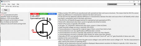
This small PEAK equipment has some basic curve tracing capabilities, but I don't have the courage to use it to check these VFETs because the setup has many voltage and current settings and I don't want to type in improper values. I have attached the screen-shots from the PC software of DCA75 below.
Do you know what the original failure of the amplifier was? You did mention the bead diodes being open...
In fact, I should remeasure them by removing them from the PCB. I just did a quick check and they didn't behave like diodes, they were showing In the circuit in one polarization they all measure around 3.5megs and in the other direction about 50 to 100 ohms.
I haven't powered up the amplifier myself, but the previous owner was ambitious to show that it was "working". So, I saw the lights of the PPM at zero for both L and the R channel.
Attachments
Do you know what the original failure of the amplifier was? You did mention the bead diodes being open...
I started de soldering the "death diodes" from the PCB and measuring them with the PEAK DCA75. They are not behaving the same as they do in circuit and I am receiving the following from the measurement results:
Channel A:
Vf=1.37V at 5mA
Vf=1.36V at 5mA
Vf=1.34V at 5mA
Channel B:
Vf=1.31V at 5mA
Vf=1.31V at 5mA
Vf=1.31V at 5mA
I presume it is again me, not being able to tell whether a diode is functional or not by measuring it in circuit.
A high channel resistance gives functional stability and low distortion.
The electrical and thermal properties of the VFET architecture are different from the properties of the heavily doped, strongly nonlinear P-N junction diode.
For devices in audio use, depletion mode is preferable from a qualitative point of view.
Driving VFETs (output devices in general) by a common-emitter amplifier could be a desirable objective.
The implementation of a switching push-pull VFET amplifier requires a great deal of theoretical and practical consideration.
- Home
- Amplifiers
- Solid State
- Got a Sony TAN-8550 with fried 2SJ18s, now what?