May be none but you seem eager to know, also you say you have seen everything and that also know the same, why do you think you have those hum problems?
If you need to add more capacitance in the rails, it certainly has to be because de PSSR, dont you think?, also you may have problems with grounding,
Cheers.
If you need to add more capacitance in the rails, it certainly has to be because de PSSR, dont you think?, also you may have problems with grounding,
Cheers.
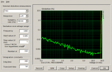
In my posting #133 you find the details and the background information. As the modification of the filter caps killed the hum with input shorted I consider this specific problem solved. There are loads of other sources of hum disturbance possible depending on grounding, and sometimes I observe strange effects when I modify the wiring of the test setup. So this mod just fixed ONE source of possible hum disturbances - others may follow...
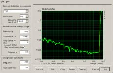
Always keep in mind that I measure very small disturbances in the uV-range here.
Always keep in mind that I measure very small disturbances in the uV-range here.
Let us play around with the numbers.
starting with 1W/8Ohm corresponds to 2,8Vrms=9dBV
thus a hum level of -115dBV is -124dB below 1W
A high efficient pa speaker box with 100dB/1W sensity at 1m distance driven with that voltage outputs
100dB-124dB = -24dB hum sound level at 1m distance.
This is a sound level 24dB below any audibility - ignoring the fact that hearing sensitivity drops significantly at 50Hz.
Meanwhile the new pcbs were in my postbox. Besides re-routing the driver circuitry I had added some decoupling MLCCs and two LEDs in series with the clipping clamp diodes. First these increase max gate drive voltage 2~3V above the power rails reducing the voltage drop of the power MOSFETs.
Second they flash when clipping occurs - a practical free gift.
A first check took place - and surprise, surprise - it oscillates at 200MHz. The new design had not changed anything to that. So I investigated more time to locate the culprit. To do this I monitored the output with my oscilloscope and used an isolated test prod to probe the circuit traces. Most sensible was the neg aux supply track, here the result changed dramatically over a length of some cm. So I assumed this track to be the inductor of the resonant tank I was looking for. To dampen this it is good practice to break the loop by inserting some ferrite bead. Doing so with a 0603 bead (600Ohm @100MHz) tamed that oscillation. I added a 2n2 MLCC blocking cap behind that bead and did the same on the pos side. I conclude there has been some need of a RF decoupling filter between the driver circuitry and the gate driving emitter followers.
Last edited:
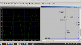
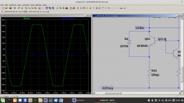
The main reason obviously was overdrive recovery of the hi-speed/low voltage BJT (BC850C) driving the VAS cascode (DZT5551). Besides some fine-tuning of compensating networks (a never ending story) I replaced the BC850C by a low signal NMOS 2N7002 hoping to improve recovery from overdrive. This was a 1:1 replacement without any adjustment of DC biasing: Output DC offset measured 5mV after this patch. All in all there is no reason not to put such NMOS into this very position.
Attachments
Last edited:
Aiming to extend full power bandwith to 1MHz the output snubber is a bottleneck that must be removed. Some experiments revealed that self-oscillation can be prevented w/o snubber with two 100pF capacitors parallel to gate-drain terminals of the power MOSFETs. I assume this cleans out voltage-dependent capacitance of MOSFETs as a source of instability.
Last edited:
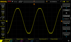
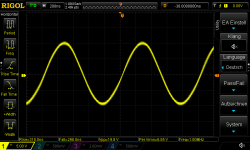
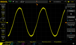
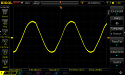
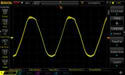
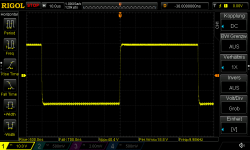
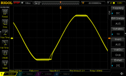
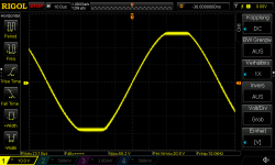
1MHz sinewaves of 20/30/40/50Vpp measured at output, loaded with 10R dummy. There is some visible distortion at high levels. This depends directly of the gate series resistors. After some fiddling I choosed 330R/220R as the best looking compromise. This is an obvious improvement comparing with the results presented in posting #92 from 2019-08-15.
Attachments
Last edited:
Mains power consumption was 47W with 1MHz 50Vpp into 10R dummy, dropping to 40W w/o dummy load.
I conclude that the series inductance of the dummy load takes over at 1MHz reducing current to a fraction of the nominal value.
40W power consumption w/o dummy load indicates significant losses inside the amp, presumably cross-conduction.
There may be some room of improvement by further optimizing gate drive circuitry.
On the other hand - these lateral FETs handle such abuse without any problems - BJTs would have blown during the fraction of the first second.")
I conclude that the series inductance of the dummy load takes over at 1MHz reducing current to a fraction of the nominal value.
40W power consumption w/o dummy load indicates significant losses inside the amp, presumably cross-conduction.
There may be some room of improvement by further optimizing gate drive circuitry.
On the other hand - these lateral FETs handle such abuse without any problems - BJTs would have blown during the fraction of the first second.
Last edited:
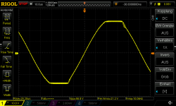
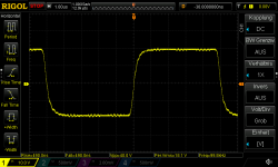
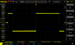
Actual measurements of square response with 1/10/100kHz
Attachments
Last edited:
I have been fighting with a slight overshoot all the time - and LTSpice confirmed this behavior. Increasing the input LP filter as a compensation is a poor workaround here. At the end it helped to over-compensate the feedback divider by increasing the lead cap from 33pF to 47pF. This can be understood as some "partial cherry compensation".
Last edited:
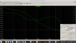

So asked LTSpice - and, voilà, the same misbehavior shows up in simulation. The VAS input voltage rises upto 40V referred to neg supply rail - this is an excessive overdrive that takes time to recover.
This issue relates to swapping the VAS BJT to 2N7002: The BJT-base limited the VAS input level, the NMOS gate does not.
This issue relates to swapping the VAS BJT to 2N7002: The BJT-base limited the VAS input level, the NMOS gate does not.
Attachments
Last edited:
- Home
- Amplifiers
- Solid State
- Just another lateral FET amp