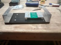
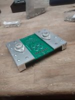
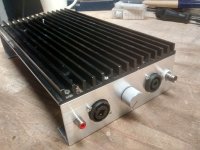
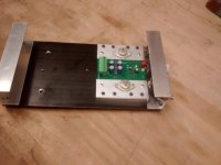
Now there is some work in progress....
Attachments
-
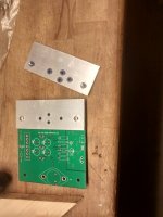
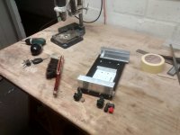 01_workbench_IMG_20190730_120300139_HDR.jpg161.5 KB · Views: 606
 -
 06_ensemble_IMG_20190730_184252325_HDR.jpg157.1 KB · Views: 344
 -
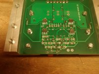
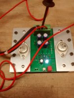
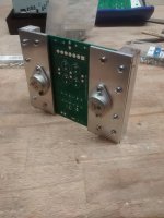 05_module_IMG_20190730_183420593.jpg124.7 KB · Views: 609
 -
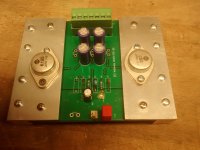
 04_module_IMG_20190730_183249167.jpg120.6 KB · Views: 597
 -
 03_heat_conductor_IMG_20190730_125432546_HDR.jpg113.8 KB · Views: 583
 -
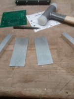 02_heat_conductor_IMG_20190730_121438313.jpg111 KB · Views: 600
I have been using JLCpcb for a while now, I think they are great for what they are worth. Cheaper than pcbway, so I am sticking with them.
I have had no data load rejections to date. I made a mistake once and caught it early enough to contact them to scrap the design before it got into production.
I can get them delivered fast with DHL express and pay duties/brokerage or the really slow way with DHL post I guess it is, but it comes via Canada Post and no brokerage/duties.
Good luck with your design voltwide, nice to see pics of your work, I can see how much more assy is required for a TO-3 metal can vs a TO-264 as I have used.
Last edited:
Thank you for the kind wording.

You can see some good reason why this case is obseleteI can see how much more assy is required for a TO-3 metal can vs a TO-264 as I have used.
Last edited:
Thank you for the kind wording.
You see a good reason why this case is obselete
I found I could use my pcb as a drill template and get very good results.
I line up pcb with heatsink then clamp pcb to heat sink.
I then drill one of the transistor mounting bolt holes.
I put a bolt through the hole and tighten it down.
I then drill opposite end of heatsink and bolt that down.
You can now drill out rest of the holes through the pcb (with care.)
I have done quite a few this way and never had a problem.
I found for the connecting wire holes a hand held drill was better to stop the drill biting in the wrong place. I put the drill through the pcb hole and start it up slowly.
They are a pain and much harder than single hole transistors but nothing wrong with a bit of nostalgia !
I cannot complain about quality - it is fine. Being a "coarse" design with much clearance requirements are relaxed and it is hard to manufacture scrap.Hi Voltwide,
How is the quality of these PCBs? I've ordered many PCBs from Chinese but there is no anywhere i actually feel OK.
Regards,
Cuong Nguyen
I do not take the pcb as a stencil but a 1:1 printout from my laser printer, which is sufficiently accurate. With paper stencil I punch-mark and then drill. This is less convenient but I avoid any ugly damage of the pcb.I found I could use my pcb as a drill template and get very good results.
I line up pcb with heatsink then clamp pcb to heat sink.
I then drill one of the transistor mounting bolt holes.
I put a bolt through the hole and tighten it down.
I then drill opposite end of heatsink and bolt that down.
You can now drill out rest of the holes through the pcb (with care.)
I have done quite a few this way and never had a problem.
I found for the connecting wire holes a hand held drill was better to stop the drill biting in the wrong place. I put the drill through the pcb hole and start it up slowly.
They are a pain and much harder than single hole transistors but nothing wrong with a bit of nostalgia !
I do not take the pcb as a stencil but a 1:1 printout from my laser printer, which is sufficiently accurate. With paper stencil I punch-mark and then drill. This is less convenient but I avoid any ugly damage of the pcb.
If you go gently the hole aligns the drill into it.
Also, using an electric hand drill with the drill down the hole before you start stops the pcb hole being widened out.
Some remarks to the actual pcb layout. Being 2-sided big copper filled areas are possible. So I divided the amp into 2 zones: the input zone with LTP ending at the input of the VAS. All nets of this area carry little voltage levels, so they are screened by a copper fill connected to analog GND.
The second zone is the power, carrying all the nets at the high output level. This includes the VAS output as well. This hole area is screened by a copper plane connected to the output. The idea behind this is to minimize the parasitic capacitive loading of the VAS by the well known method of an active screen.
The top view of the pcb shows these two areas, separated by a wide trench acting as "isolation barrier".
And this isolation barrier is bypassed by a minimized bunch of tht resistors and caps.
I use JLCPCB mostly but have used PCBWAY.
The quality has been amazing even on fine scale SMD with very small via's.
I sometimes get JLCPCB rejecting my files for silly reasons.
I just resend the same files and next time someone different scans them and they go through.
Over the years I experienced similar problems - issues caused by my file output in most cases:
- I forgot to add the edge cut layer, so the size of the pcb was unclear
- I moved the ref designators in the silk screen to my gusto - so some of them landed on pads - that have to be entirely clear. In that case the manufacturer did the clearing for me (blush!).
I did, please look at posting #4 and #7Dear Voltwide,
I want to use a different type of Heat sink. Can you kindly post your original kikad files?
--gannaji
hm - maybe both.Voltwide, is this an extension of your previous designs or did you start from scratch?
The design is not really new, just a composition of well known details. This very design started on scratch with extended LTSpice simulations that led to the current pcb layout.
I do not love that either... the part I would rather not have to do but it is a necessity or you are left with a proto and no home.
- Home
- Amplifiers
- Solid State
- Just another lateral FET amp