I don't agree. And certainly not with the negative attitude of this kind of comments, critical and negative, never offering better solutions.So many RC frequency correction groups which actually just hamper schematic's performance.
An amplifier has a lot of poles and zeros. it seems logical to compensate them by more than one.
May-I refer to Dadod's 200W amp, that has been tested and measured in real world by two well equipped contributors (Richard Marsh and astx) as stable and the best sounding amp they had heard ?
I have, on the C version, very similar results
Anyway, I had tweaked more deeply the compensation values of the C version.
It is a tricky work to set 4 amps ( version V & C, both with or without error correction compatible with the same schematic). And the stability have to be OK with and without error correction.It takes a long time to be optimised.
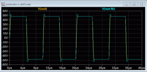
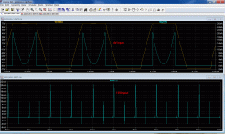
To answer the 100kHz square waves of the C version you had send to me by PM, here what I got with little changes of compensation network values. And most of the non nice looking edges of the square waves were the consequence of the different gate capacitor values of the P & N power mosfets. Setting the base stoppers to 220 & 146 ohms solved-it and increased the SR.
Input filter removed (before and after output coil).
The peak is typical of TPC and can have only benefits. it will not exists any more with the input filter in, but the amp will, for sure, have a dynamic behavior on transients, what we expect from a CFA.
Now, no need to any more argue. Everything had been done to address all the critics. We just have to wait for the PCB, build-them in real world and see on the bench what can be refined.
And I'm confident on the results.
Attachments
Last edited:
An amplifier has a lot of poles and zeros. it seems logical to compensate them by more than one.
Uh-oh. Does "dominant pole" ring a bell?
After your previous insulting message, erased by the moderation, I thought you'd understand I will never ring you, dear syn08, to give-me any lesson ?
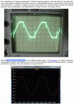
This said, as a demonstration of your mastery of feedback loops and their compensation, this screen shot of one of your design in your web site. Modestly titled "The Ultimate Audio Amp".
And the behavior of Pizzicato under the same conditions ... without any funny "clipping protection circuitry" to hide failings under the carpet.
Between you and me, can't-you find more constructive occupation than attacking other contributors, reason why you have been in my ignore list since a long time ?
Attachments
Last edited:
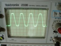
I have no idea what are you talking about, the first picture is taken from my web site (without permission, BTW), showing the output before the clipping protection was installed. You of course conveniently omitted the final result, after the clipping protection was installed. Clipping protection is hiding failings? Huh? Do you realize those are scope screenshots, not simulation BS? I guess not...After your previous insulting message, erased by the moderation, I thought you'd understand I will never ring you, dear syn08, to give-me any lesson ?
Otherwise, I am guilty as charged for insulting you by mentioning “dominant pole”. That’s a curse idiom that I should not have mentioned in this thread, I apologize. Poles should not be allowed to dominate a free spirit and should behave in any circumstance.
Attachments
Last edited:
More about the C version.
Using a 75V 50mA separate regulated power supply for the front end and VAS, will increase its power to 250W under 8 Ohms.
Just at this clipping limit, distortion is simulated at 0.000023%. (one zero less with no error correction).
An other benefit will be an increased supply ripple rejection.
That will be the solution I will chose for myself.
The only drawback i can imagine is a little increase of AC leaks, adding a transformer. But, choosing the best combination of primary phases of the transformers, it is possible that, on the contrary, they cancel a little each other.
Of course, star grounding will be a requisite.
For those that can be afraid by the 160° minimal phase turn of the OLG, notice this minimal is not worsened by any reasonable capacitive load.
The amp has been simulated with 4µF, a model of 10m of cable (lumped element) loaded by an average speaker model. And a model of this cable followed by the QUAD ESL57 speaker, reputed to be one of the most critical load to be found.
Remain rock stable.
At least we have to remember that the protection will immediately fire if the amp is oscillating.
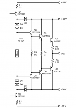
Krisfr, please, could-you add this option on your printed board (just a connector there ?). In this case the included regulator will not be populated.
I apologize for all those last minutes changes.
Using a 75V 50mA separate regulated power supply for the front end and VAS, will increase its power to 250W under 8 Ohms.
Just at this clipping limit, distortion is simulated at 0.000023%. (one zero less with no error correction).
An other benefit will be an increased supply ripple rejection.
That will be the solution I will chose for myself.
The only drawback i can imagine is a little increase of AC leaks, adding a transformer. But, choosing the best combination of primary phases of the transformers, it is possible that, on the contrary, they cancel a little each other.
Of course, star grounding will be a requisite.
For those that can be afraid by the 160° minimal phase turn of the OLG, notice this minimal is not worsened by any reasonable capacitive load.
The amp has been simulated with 4µF, a model of 10m of cable (lumped element) loaded by an average speaker model. And a model of this cable followed by the QUAD ESL57 speaker, reputed to be one of the most critical load to be found.
Remain rock stable.
At least we have to remember that the protection will immediately fire if the amp is oscillating.
Krisfr, please, could-you add this option on your printed board (just a connector there ?). In this case the included regulator will not be populated.
I apologize for all those last minutes changes.
Attachments
Last edited:
Using a 75V 50mA separate regulated power supply for the front end and VAS, will increase its power to 250W under 8 Ohms.
OMG, not for you, but for the anonymous lurkers, do you realize what is going to happen if the amp input is going to be driven, even for a few microseconds, high enough to make the output (power stage follower input) exceed the power stage power supply? I would not want to be around. You need at least some diodes to clamp the power stage input, and better move the emitter follower to the higher supply.
As of 0.00000x% distortions (meaning a few parts per billion), with or without "error correction" (whatever that is here, I have no idea, error correction as we know it is not something that one may add like icing on a cake) it's not even funny anymore, obviously you did not build and measure an amplifier with even three orders of magnitude higher distortions. And yes, this is a direct "insult" to you.
But nevertheless, have fun, simulation is free
 .
.As they need the shortest connections possible*, I believe the most flexible solution is to use a L profile. Like: L Profile Aluminum Profiles, Gypsum Aluminum Profiles, Aluminum Profiles, Aluminum Products, Aluminum Raw Materials | Hadco Metal Trading http://www.homebuilthifi.com/images/projects/325/CR02.JPGOK, what heat sink are you using for the TO-3's?
* In every case, the gates stoppers have to be as close to the gates as possible and not wire bound (not inductive).
OMG, not for you, but for the anonymous lurkers, do you realize what is going to happen if the amp input is going to be driven, even for a few microseconds, high enough to make the output (power stage follower input) exceed the power stage power supply? I would not want to be around. You need at least some diodes to clamp the power stage input, and better move the emitter follower to the higher supply.
As of 0.00000x% distortions (meaning a few parts per billion), with or without "error correction" (whatever that is here, I have no idea, error correction as we know it is not something that one may add like icing on a cake) it's not even funny anymore, obviously you did not build and measure an amplifier with even three orders of magnitude higher distortions. And yes, this is a direct "insult" to you.
But nevertheless, have fun, simulation is free
First, please, learn to read a schematic. During this time, we will be safe from your rolling hate and insults.
"For the anonymous lurkers", a quick look at the attached picture demonstrate that what syn08 pretends is totally wrong, false, dishonest.
The voltage at the base of the drivers will be max ... 70V. And at the gates, one diode junction ...under. And let see the current at the base of the driver too (it begins to conduct like a diode): 21mA max. No need for any resistance.
For sure syn08 ignore that the base current rating is 1/3rd the Collector current ? And, here, the peak current limit of the transistors used are... 200mA.
What will happen ? Nothing. The protection will fire before this point will be reached and will cut the input signal. And you will not even be assaulted by the awful distortion.
Anyway, the expensive power Fets are here protected by the drivers. If something burn (usually cut in this situation)) it will be the cheap drivers: not the apocalypse syn08 describe.
This is one of the reasons why i had not put the drivers at the VAS supply. The other one would be insulting (or instructive ;-) to syn08. I don't wanted to use 50 active devices like him. 26, it's already too much. One of the first thing we are taught in electronic is "simple is beautiful". And I'm not sure that his "ultimate" amp will survive neither at 1000V applied to inputs, or everywhere else. Pizzicato neither, for sure ;-) But reasonably safe ? I'm confident.
BTW: syn08, have-you been abused by a simulator when you were a child, that could explain most of your behavior troubles ? I'm sorry, it is impossible to measure an amp that is not already build. or may-be you have a solution ?
Please stop polluting this thread, harassing-me the way you do, enough is enough. It does nothing good to your image and it does not help anyone. Unless - a miracle is always possible ? - you will have something positive to bring ?
Just the contrary. It is the first time I design totally an amplifier with a simulator, leaning to use-it in the same time. And, go figure, I designed (to be honest we were two working together on the design in the R&D office, with other draftsman and mechanics) my first commercial amplifier (2X50W), sold at thousands of units, 50 years ago. You were probably not born at this time (and, if yes, you are just a really sour old man). And, go figure, it measured 0.025% distortion. Be assured that, when it will be on the test bench, it will be measured and tested for safety by all the possible way. And modified, if any need, at this time. No computers neither.obviously you did not build and measure an amplifier with even three orders of magnitude higher distortions. And yes, this is a direct "insult" to you.
Sorry to have to explain to you that we are not at this point, right now. But at the schematic before the first prototype. If I understand well, it is a bad practice because you build first and design ... after ? Assembling parts of schematics and ideas of other designers picked here and there ? But that is enough. PLEASE LEAVE US ALONE and go insulting somebody else elsewhere as it is obvious you are not interested by this project.!!!
Attachments
First, please, learn to read a schematic. During this time, we will be safe from your rolling hate and insults.
"For the anonymous lurkers", a quick look at the attached picture demonstrate that what syn08 pretends is totally wrong, false, dishonest.
The voltage at the base of the drivers will be max ... 70V. And at the gates, one diode junction ...under. And let see the current at the base of the driver too (it begins to conduct like a diode): 21mA max. No need for any resistance.
For sure syn08 ignore that the base current rating is 1/3rd the Collector current ? And, here, the peak current limit of the transistors used are... 200mA.
What will happen ? Nothing. The protection will fire before this point will be reached and will cut the input signal. And you will not even be assaulted by the awful distortion.
Anyway, the expensive power Fets are here protected by the drivers. If something burn (usually cut in this situation)) it will be the cheap drivers: not the apocalypse syn08 describe.
This is one of the reasons why i had not put the drivers at the VAS supply. The other one would be insulting (or instructive ;-) to syn08. I don't wanted to use 50 active devices like him. 26, it's already too much. One of the first thing we are taught in electronic is "simple is beautiful". And I'm not sure that his "ultimate" amp will survive neither at 1000V applied to inputs, or everywhere else. Pizzicato neither, for sure ;-) But reasonably safe ? I'm confident.
BTW: syn08, have-you been abused by a simulator when you were a child, that could explain most of your behavior troubles ? I'm sorry, it is impossible to measure an amp that is not already build. or may-be you have a solution ?
Please stop polluting this thread, harassing-me the way you do, enough is enough. It does nothing good to your image and it does not help anyone. Unless - a miracle is always possible ? - you will have something positive to bring ?
WTF are you talking about? It seems like techno babble to me, referring an unexplained simulation, a protection that’s nowhere to be found (protecting against what?) and to add insult to injury you don’t seem to grasp the effect of a forward biased base-collector transistor junction (the emitter follower) and babble about some unknown/undefined currents, 21mA then 200mA. Base current rating 1/3 of the collector current rating, WTF, who taught you that?
You sir are hopeless. I only feel for those very few that are still wasting their time in this thread.
You sir are hopeless. I only feel for those very few that are still wasting their time in this thread.
On a positive note, those still involved will have a unique learning experience!
Jan
WTF are you talking about? It seems like techno babble to me, referring an unexplained simulation,
Current at the base of the driver, that Flows across the collector because the reverse bias. A situation that happens frequently with inductive loads.
Ie(Q11) on the picture was not talkative enough ?
What else ?
Obviously you had not read the thread and don't know what we are talking about. So you are talking about what ?a protection that’s nowhere to be found (protecting against what?)
A quick search in Google ? the first link is, by example:and to add insult to injury you don’t seem to grasp the effect of a forward biased base-collector transistor junction (the emitter follower) and babble about some unknown/undefined currents, 21mA then 200mA. Base current rating 1/3 of the collector current rating, WTF, who taught you that?
What is the maximum rating of the Base current? |FAQ|ROHM Semiconductor
I was asking you, several times, that YOU stop wasting your (and our) here.You sir are hopeless. I only feel for those very few that are still wasting their time in this thread.
One other post obviously against the rules. I hope the moderators will take sanctions against this guy, It is impossible to continue in this atmosphere.
The attitude of this guy, his harassment, his insults and his hate against somebody he don't know at all is not acceptable. And I'm not the only one that the guy attacks this way: it is his usual behavior.
This said, the guy is not totally wrong in theory, and I will surely not do the same with the V version, that is less limited in VAS current .
The amp is in progress, and, here, I was just showing what we could expect on power and distortion from an increased voltage of 5V at the front end.
As explained from the beginning, it is a work in progress, and the final schematic that is supposed to come with the printed board after built and tested with real components.
A normal and polite behavior should be to have wrote something like "
Tournesol, don't you think there is a risk that the driver can be in reverse bias when the amp is heavily clipping ?".
This said, I had verified that, in this particular situation even with a 65V voltage in the power stage, (PSU non regulated heavily loaded) we were in the SOA for the driver. And, after verification in the V version, yes, the collector has to be moved to the 75V power supply (If we decide to keep this option that add only 1dB).
Please Jan Didden , make the test yourself in your home, with a cheap NPN transistor, 10% more voltage on the base than on the collector, 1Meg (mos fets) in the emitter and a base current limited at 10% of its SOA max normal current. Then came back and tell-us, honestly, if the device has been burned. ? And, if yes(I should be surprised), how long it had took to fry the transistor ?
Last edited:
Well, Tryphon,
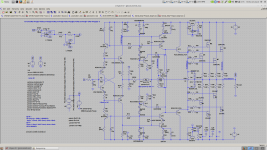
I don't want to be thrifty (as I've already told you), that's why I'm suggesting you to implement a Baker clamp in your schematic, see attached picture. It is for V6 actually but implementation in "c" version will be completely the same.
I don't want to be thrifty (as I've already told you
), that's why I'm suggesting you to implement a Baker clamp in your schematic, see attached picture. It is for V6 actually but implementation in "c" version will be completely the same.Attachments
May-be a good idea. I don't have a lot of free time, those last days, and I'm on the power supply. Give-me a little time to look more deeply at what it brings. I was thinking yersterday to a baker on the drivers.Well, Tryphon,
I don't want to be thrifty (as I've already told you
You know I'm a little miser on the numbers of active devices ;-)
Thanks a lot, arpagon, for your suggestion: It is now on my to do list ;-)
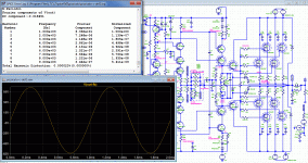
It's interesting that the output amplitude is limited to ~53V no matter what is the input signal and the voltage gain of the stage. It means you cannot have more than 175W/8 Ohm no matter what power supply voltages you have.
And this is the reason the Baker clamps to not work as supposed (schematic behaves itself so good that exit from clipping without any fuss).
And this is the reason the Baker clamps to not work as supposed (schematic behaves itself so good that exit from clipping without any fuss).
5V of losses Mosfet side, and the zener limit the VAS supply to 65V. Plus the two diodes in the VAS, plus the cascode, plus the driver .... Reason why I'm exploring a separate PSU for the front end.
My actual version with the internal regulator goes up to 58V, and 61V if you just remove the zeners in the cap multipliers in your version . ;-)
But there no actual problem I can see with the clipping in all those cases...
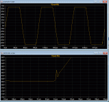
Now, always in version V, with a front end powered at 75V (setting the driver collector there, in this case, your clamp works nicely as expected. But (see attached) the amp itself is pretty clean. Only a little pic immediatly damped. So I don't know if it is worth the pain and the added complexity of two extra active devices.
Specially while there is no issue with the C version.(Not to forget the protection that do not allow clipping by design ;-) What do-you think about ?
My actual version with the internal regulator goes up to 58V, and 61V if you just remove the zeners in the cap multipliers in your version . ;-)
But there no actual problem I can see with the clipping in all those cases...
Now, always in version V, with a front end powered at 75V (setting the driver collector there, in this case, your clamp works nicely as expected. But (see attached) the amp itself is pretty clean. Only a little pic immediatly damped. So I don't know if it is worth the pain and the added complexity of two extra active devices.
Specially while there is no issue with the C version.(Not to forget the protection that do not allow clipping by design ;-) What do-you think about ?
Attachments
Last edited:
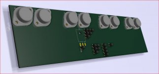
Hehe !Coming soon for TO-3's aficionados
Tried a classical 2 diodes Baker clamp on the VAS amp transistor in the 250W V version. Works perfect. BUT ... Increase distortion by near a 10 factor.
So I think we can live without. On my opinion, it should be stupid to sacrify performance in normal use for a little beauty of the square waves when it clips.
Arpagon, BTW, your schematic gives better results than the 2 diodes clamp. Half the distortion. But still increase (without/with) from 0.000074 to 0.000273%.
But I will follow your preferences and suggestions.
Krisfr, sorry for again a little change, but contrary to the C version that has less base current in case of hard clipping, the Version with a separate higher front-end voltage request absolutely to move the driver collectors to the same line than the VAS power supply.
I don't know what exactly is your arrangement but have you tried something like this?Hehe !
Tried a classical 2 diodes Baker clamp on the VAS amp transistor in the 250W V version. Works perfect. BUT ... Increase distortion by near a 10 factor.
Attachments
- Status
- This old topic is closed. If you want to reopen this topic, contact a moderator using the "Report Post" button.
- Home
- Amplifiers
- Solid State
- Pizzicato, a 200W low distortion CFA amplifier