I don't know, Krisfr. What is your opinion ? I thought on a separate little board to let users to chose or not protection etc... ?1-Where will the additional parts go?
2-Also how do you want to make the 12 volts, with resistor zener and cap?
I think it would be better to add a separate litle psu for 12V's. That come, by habit with SMPS, by example. And keep the amp itself simple ?
This way it will be used for whatever we want for comfort: Remote, soft start, silent stop, fans, temperature sensors and fan command if any, etc. without any impact on the PSRR.
BTW, may-be it should be careful, on your schematic of OPAMPS, to add a comp cap in parallel with the feedback resistance of the "2", just in case ?
Last edited:
One thing to have in your back pocket is the temperature compensation for the input stage. The zeners have a tempco of around -2mV. A blue diode is double this. An investigation of different input devices hasn't been made yet. It does appear the input stage has quite a bit of sensitivity regarding change of device.
The concept of the input is to have the same current operating in both transistors of the cascode. Change of device easily generates an imbalance.
The concept of the input is to have the same current operating in both transistors of the cascode. Change of device easily generates an imbalance.
Spladski, thanks A LOT.One thing to have in your back pocket is the temperature compensation for the input stage.
I just tried a step temp simulation in LTSPICE. You are right, the bootstrap is catastrophic and need to be addressed.
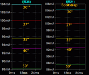
Between 0 to 50°, while the current source only vary form 1.22mA to 1.18 mA, the cascode current goes from 44mA to 0mA, the driver current goes from 90mA to 0, and the output devices current from 750 to 0 mA.
I cannot believe-it !
Surprised, because, apart this front end, it is a topology I'm used to, IRL, without major issue.
All helps appreciated.
Krisfr, I think it is necessary to fix this major issue before going further in the board design.
Last edited:
So, at the end, bootstraping the input stage was a false good idea. Back to the original design with the addition of the traditional biasing transistor.
As the HEX and Lateral Power FETS stabilize themself around 100/150mA, it has not to be on the PowerFETs cooler.
The advantage is that in case of a bad contact of the adjustable resistance, the bias will decrease.
A simple diode had been added to the current sources zeners to give them tempco.
Like this it is over compensated. I still have to see how it behaves without them but with the biasing transistor alone.
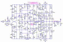
The schematic will be something like this, I still have to refine the current values and optimize feedback compensation network.
Schematic under, just to give an idea.
As the HEX and Lateral Power FETS stabilize themself around 100/150mA, it has not to be on the PowerFETs cooler.
The advantage is that in case of a bad contact of the adjustable resistance, the bias will decrease.
A simple diode had been added to the current sources zeners to give them tempco.
Like this it is over compensated. I still have to see how it behaves without them but with the biasing transistor alone.
The schematic will be something like this, I still have to refine the current values and optimize feedback compensation network.
Schematic under, just to give an idea.
Attachments
Last edited:

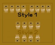
How about Style 1 but with alternating adjacent P and N devices?
mlloyd1
mlloyd1
Okay, I will work on the output area and wait for the front end later.
Please choose a layout style to use for the output area.
Thanks
How about Style 1 but with alternating adjacent P and N devices?
mlloyd1
Exactly !
1 -Thanks, LKA.1 -Very nice amp and results.
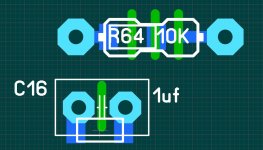
2 -I don't like compensation C16,17.
3 -Btw, can you beat this ?
200W/4R (VFA TMC+CHERRY+EC) less than 1dB under clipping
2- I don't like-it neither, but not found a better way.
3- Certainly not with a CFA ;-) (Congratulation. Any link to the thread ?)
Last edited:
The style I is better for cooling and thermal balance. If placed at 1/3 -2/3 from the bottom of a passive cooler, it allow the best cooling efficiency.Please choose a layout style to use for the output area.
But style 2 is, may be, easier for you, and allow shorter connexions to the Power devices ?
On my side, I tend to prefer the 1.
About the front end, I have a question.
If we stay with the non bootstrapped input stage version which seems more stable with temp variations (I have to ensure more deeply) What do-you (all) think about putting adjustable resistances R3, R4 to adjust the currents to 1.2mA in the second stage whatever the VBE mismatches ?
I will do style 1 and put in jumpers to allow for variations of certain schemes, such as one or two drivers and either smd or tth devices, as well as test points for easier development. This is going to be a development type board. All suggestions are welcome and desired. Should another thread be started for the layout of the board? I will do alternating n and p channels of the output devices.
You can forget the two drivers. No need, spladski and I we both agree.I will do style 1 and put in jumpers to allow for variations of certain schemes, such as one or two drivers and either smd or tth devices, as well as test points for easier development. This is going to be a development type board. All suggestions are welcome and desired. Should another thread be started for the layout of the board? I will do alternating n and p channels of the output devices.
About SMD or TTH, you have to chose, on my opinion: What should be the interest to go for SMD if the board is large enough to support TTH, what do you think ?
After further simulations, it appears that the bootstrapped version gives the same tempco than the original one. See attached. Quite secure. So we will finally keep on this one.
I tried simulations with 3 different input pairs. Nothing catastrophic. I let R3 & R4, in case the VBE will have too much differences.
Time for a little rest for me.
I tried simulations with 3 different input pairs. Nothing catastrophic. I let R3 & R4, in case the VBE will have too much differences.
Time for a little rest for me.
Attachments
Dear Krisfr,
https://cdn.shopify.com/s/files/1/1006/5046/files/universal-mounting-specification-v2.1.pdf
--gannaji
https://cdn.shopify.com/s/files/1/1006/5046/files/universal-mounting-specification-v2.1.pdf
--gannaji
After further simulations, it appears that the bootstrapped version gives the same tempco than the original one. See attached. Quite secure. So we will finally keep on this one. I tried simulations with 3 different input pairs. Nothing catastrophic. I let R3 & R4, in case the VBE will have too much differences. Time for a little rest for me.
Hi Tryphon, I haven't had much time to pop in and will try to catch up with what is happening next few days. WRT IP diamond pair, you can use either bootstrapped or non bootstrapped and jig them to have whatever tempco you like. I suggest you dump the sim and breadboard the front end up, just the diamond pair and do some real measurements. Use a hot air gun for heat source. Here are a few tricks: - You can use diodes in place of R10 and R25. R1 and R3 will have to go bigger to achieve same current. If diodes are coupled to IP BJT's, you will end up with negative tempco.
- Second trick is to play with resistor sizes. IOW if R1/3 are smaller than R10/25 and the BJT's are thermally coupled, it should have a negative tempco.
- One of the issues impacting thermal stability is you have current gain in the voltage stage because of ratio of R5/31 and R12/26 = 820/25. So any thermally induced current run away in IP stage gets magnified through 2nd stage.
- A solution to this is to make R5/31 and R12/26 more similar in size. This will lower your current gain. The downside is distortion will go up a bit. You can get around the distortion issue at high frequencies by bypassing R12/26 with a film cap (and usually a smaller series R). This will increase OLG at higher frequencies. Since the amp has such low distortion at 1kHz it's not too much of an issue to increase distortion at these frequencies.
- I'll run the sim when I get some time. I haven't got my head around the error correction yet, need to have a closer look. Doing sims with opamp based error correction is pretty unreliable.
The amp looks great so far.
T
Terry preempted. This version is more tolerant of device change and temp. Split the driver resistor so that a feedback point can be taken midway without output devices to establish DC conditions.
Attachments
I believe that will go the opposite way, IOW, will make it *more sensitive to temperature rise. Diodes should go in input pair circuit in place of R4 and R7. You can also use schottkys for a smaller voltage drop.
I cannot stress enough the need to actually breadboard these circuits and measure them. You learn a lot on Ltspice but more building the circuit.
I cannot stress enough the need to actually breadboard these circuits and measure them. You learn a lot on Ltspice but more building the circuit.
- Status
- This old topic is closed. If you want to reopen this topic, contact a moderator using the "Report Post" button.
- Home
- Amplifiers
- Solid State
- Pizzicato, a 200W low distortion CFA amplifier