Sorry, Sajti, it was your suggestion.Apologies.One of them to use some That300 with Mark's suggestion.
When I said for the funAs this protection is extracting the difference between input and output signals, I will explore some added error correction, at this time and for the fun, from the same circuit. What do-you think ?
I'm on this at this moment.
See attached:
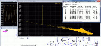
At 10KHz, got 0.000052% of HD
Of course it is totally unrealistic. A LTSPICE hallucination.
Attachments
Last edited:
No problem! You got many ideas to try...
Anyway I don't like THAT, because of the low Hfe. I use BC550C/560C, cascoded with 2N5551/5401, or fully KSC1845/KSA992 in my amplifier. Matching is necessary, but not hurt so much.
0.000052% is just a dream. But You can get some 0.001% in real life.
Sajti
Anyway I don't like THAT, because of the low Hfe. I use BC550C/560C, cascoded with 2N5551/5401, or fully KSC1845/KSA992 in my amplifier. Matching is necessary, but not hurt so much.
0.000052% is just a dream. But You can get some 0.001% in real life.
Sajti
At 10KHz, got 0.000052% of HD
you can simulate .... it is not easy to build a real amp which measures below 0.001% at any power level (4R,8R) in whole audio band
Transistors are like food in the supermarkets. Dozen of similar products under different brands and, often, not what we need.
To match transistors is not something easy for a DYIer because it requires a great number of samples. And not a fun for a manufacturer because it is time consuming.
To match transistors is not something easy for a DYIer because it requires a great number of samples. And not a fun for a manufacturer because it is time consuming.
Write out a little homework problem in mathematics and solve it. The answer is reassuringly good.
You have an envelope containing 100 transistors. Each transistor's VBE @ Ic=2mA is guaranteed to be in the range (0.63V < VBE < 0.68V). If you accurately measure all 100 transistors and record their VBEs, you can find the two transistors whose VBEs are closest together. The "best match". Question: what is the absolutely worst possible result, the "best match" with the greatest difference in VBE?
You have an envelope containing 100 transistors. Each transistor's VBE @ Ic=2mA is guaranteed to be in the range (0.63V < VBE < 0.68V). If you accurately measure all 100 transistors and record their VBEs, you can find the two transistors whose VBEs are closest together. The "best match". Question: what is the absolutely worst possible result, the "best match" with the greatest difference in VBE?
Tryphon, very nice work.
I am dabbling with a bridged CFA design after having tried many different amplifier topologies and not being totally happy with the sound.
WRT the input pair, you may have to use emitter degenerating R's to Q1 and Q5 but it may also be happy without them, it's just something to keep an eye on.
WRT the input pair Q2 and Q6 bootstrapped collectors - some people like it, some don't. It's all part of your own recipe")
Having said this, you have to be careful with bootstrapped BJT's WRT oscillation. It's relatively easy to prevent with some resistance in the collector circuit to decouple them and sometimes also a small C to ground.
One big advantage of the bootstrapped input pair is it will enable much higher source impedance drive without a significant distortion penalty. This is a good thing if you are driving the amp from a passive pot, for example.
If you run the amp 10 or 20kHz sims with a source Z of 10k, the distortion results will show this up.
I like the fast BJT's, Q13 and Q14 BJT's driving OP MOSFets. This is one reason the distortion is low, especially at high frequencies. It isolates MOS capacitances from VAS.
Should be a great amp.
T
I am dabbling with a bridged CFA design after having tried many different amplifier topologies and not being totally happy with the sound.
WRT the input pair, you may have to use emitter degenerating R's to Q1 and Q5 but it may also be happy without them, it's just something to keep an eye on.
WRT the input pair Q2 and Q6 bootstrapped collectors - some people like it, some don't. It's all part of your own recipe
Having said this, you have to be careful with bootstrapped BJT's WRT oscillation. It's relatively easy to prevent with some resistance in the collector circuit to decouple them and sometimes also a small C to ground.
One big advantage of the bootstrapped input pair is it will enable much higher source impedance drive without a significant distortion penalty. This is a good thing if you are driving the amp from a passive pot, for example.
If you run the amp 10 or 20kHz sims with a source Z of 10k, the distortion results will show this up.
I like the fast BJT's, Q13 and Q14 BJT's driving OP MOSFets. This is one reason the distortion is low, especially at high frequencies. It isolates MOS capacitances from VAS.
Should be a great amp.
T
Thanks, Terry. Could-you elaborate a little more ?Tryphon, very nice work.
WRT the input pair Q2 and Q6 bootstrapped collectors - some people like it,
some don't. It's all part of your own recipe
Good remark, if based on your own experience (that I don"t have on my side).Having said this, you have to be careful with bootstrapped BJT's WRT
oscillation. It's relatively easy to prevent with some resistance in the
collector circuit to decouple them and sometimes also a small C to ground.
I hope so, with your help ;-).Should be a great amp.
The original design was based on things I know working and sounding very well for real. Now, you kindly address some possible problems with the nice spladski's improvement. As I'm not experienced with it IRL, may I ask-you up to propose a 'practically adapted to this amp' solution with a sim file to the possible flaw you seem to fear about ? And we could see the price to pay for-it ?
Let's advance together: Improvements, solutions, keeping-it in the collaborative and positive spirit of building a project together ? When we will be at the stage of designing a board for-it, it would be better to have foreseen all the possible worries.
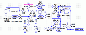
Right now, I'm exploring this idea: Error correction (optional) and protection. Using the differential signal that contain only errors due to the amp, including DC ones to improve the DC servo. (Faster and less impact of residual audio signals).
Apologies for my poor English.
The new servo-error correction seems to work. But Ltspice seems to turn crazy with the AC analysis.
The signal from input of the amp (after the input cap if any) enter in "Prot+"
The Power amp output signal (before the coil) enter in "Servo-in". And is carefully reduced in level with the R9 resistance to equal the input level one.
The OPA (fet) U2 makes the difference between the two signals. This contain only the errors produced by the amp (distortions+offset) + a very little residual from the in and output signal due the phase turns (90°).
From this point, the error signal is amplified by U1 before to return (attenuated by the R10 resistance), to the virtual - input of the amplifier (the middle point between the 2 emitters ). It adds a feedback gain without touching to the closed gain one. It is attenuated by the bridge between R10 and R34(23 Ohms) of the power amp.
To get an idea of the discrimination, once amplified by the two OPAs, the residual signal for a 1V input is 0.5mV, with the DC offset error signal of the same order.
To get an idea of the efficiency, it decreases the distortion by something like 10dB.
From the output of U1, the same error signal is filtered to get the DC (~12dB/oct above 1Hz)) and amplified to compensate the offset (DC servo).
It return to the same point.
The difference with a classical servo is that the offset is kept the same, while the signal was near totally canceled by the first differential OPA.
Attached the sim file of this part, for those who are better than me (and patient). To be added to the amp ASC itself.
Edit: The voltage source V3 was added for measurements and need to be removed)
Here the last version of the Amp itself.
Comments and critics are welcome at this step (I took previous remarks into account).
And one question. I always used Power FETs with gate stoppers. But, here it seems to act the contrary than expected. The gain loop is better without the Pick they brings. Is the Colpitts oscillator that those stoppers are supposed to dump is not simulated by LTSPICE ? If we manage to put the driver emitter very close to the gates, is-it possible to get rid of them ?
Attachments
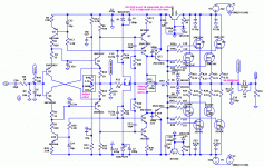
The 1MHz version
The 'out' label is shorted to 'servo-in'. Insert 1R into 'out' to separate.
The goal for the 1Mhz version was to achieve less than 1% distortion at 1MHz before the inductor. The load side reduces harmonics.
Using thick ceramic spacers for the power devices reduces parasitic coupling with the heatsink.
Attachments
If I have understood well, the problem with power FETs is the resonant circuit made by the inductive path to their gates and their capacitances (That varies with the signal).The 'out' label is shorted to 'servo-in'. Insert 1R into 'out' to separate.
The goal for the 1Mhz version was to achieve less than 1% distortion at 1MHz before the inductor. The load side reduces harmonics.
Using thick ceramic spacers for the power devices reduces parasitic coupling with the heatsink.
I remember an amp (very unstable) that was using those parasitic capacitances as the dominant pole with no miller cap.
Tried this on this one. Got a Middlebrook curve that was looking OK, loop gain up to 10KHz, with good margins etc... But no way to succeed the trans.
Sometimes LTSPICE do not help ;-)
Several questions about your last version.
- Are-you not afraid of the dissipation of the VAS devices and drivers ?
- Why the use of two caps multipliers ?
- Do-you think two drivers are really necessary ? Yes, it is easier to deal with those f... gates capacitances at very HF, but... in the audio range ?
Yes those ceramic spacers are a must. Very low thermal resistances, very good isolation and no risk of short circuit.
I tried with only one, i got around 1% as well. I think there is no need to add more transistors. What do-you think ?- Do-you think two drivers are really necessary ? Yes, it is easier to deal with those f... gates capacitances at very HF, but... in the audio range ?
I haven't had oscillation issues using Exicon laterals and 2SK/2SJ types.
The extra cap multiplier was a drawing convenience.
LTspice is optimistic so the extra predriver was to ensure proper drive of the power FET capacitance. It is your discretion.
The 1K input resistor introduces too much noise. The value should be as low as possible.
The Zobel is historic. It is not needed in a good design and can worsen PM. The current thinking is to use it on the load side of the inductor for cable termination with a similar one at the speaker.
There is further optimization. The dissipation can be reduced in the predriver.
Last edited:
Cordell Models ?I haven't had oscillation issues using Exicon laterals and 2SK/2SJ types
The Low pass input filter as well as the blocking cap are a requisite, on my point of view. The cap to ensure no change of DC offset whatever the source. Of course, the input resistor introduce both noise and double distortions. But, here, I think source side.The 1K input resistor introduces too much noise. The value should be as low as possible.
Anyway, as long as the hiss, hum and distortions are not hearable, I don't worry about shining numbers ;-)
I totally agree and don't change nothing during during sims. They are there for safety in the future printed board: Better to have empty places for components than ugly mods if any problem, don't you think ?The Zobel is historic. It is not needed in a good design and can worsen PM. The current thinking is to use it on the load side of the inductor for cable termination with a similar one at the speaker.
Do-you have valuable models for them ? Anyway, I don't think it should be a good idea to use SMD devices for VAS and drivers ;-)Would you substitute ZTX957 and ZTX857 for the 1381 3503 transistors in your testing. Ostripper indicated that these will be the future SMD devices to replace the 1381/3503's.
Thanks
Be aware that the Cordell models for lateral MOSFETs are very, very crude. Likely good enough for determining the bias point, but for stability and distortions... not a chance.
They lack some parasitic elements (notably the serial gate resistance), while not having the subthreshold region modeled makes any distortion simulation look like a bad joke.
To the best that I am aware of, the subthreshold region was never modeled for laterals; however, the models below are as accurate as you can get for a lateral MOSFET with parasitics. They are for 2SK1058/2SJ162 but Cordell models are the same for 2SK134 and 2SK1058, anyway.
The only MOSFET models including the subthreshold region modelling are for the vertical MOSFET 2SK1530/2SJ201. A former member (Andy C) made lots of effort to code these models. They are excellent and accurately predict the distortions, but these are vertical MOSFETs (need temperature compensation) and they are now extinct... No idea why Cordell did not include these advanced models in his file.
I know the Cordell models (both bipolar and JFET/MOSFET) are very popular among DIYers, but be aware they are not necessary accurate when it comes to distortion simulation. That's because they don't have advanced features (like the subthreshold region for JFET/MOSFET) coded in.
Code:
----------------------------
.SUBCKT 2SK1058 10 20 40
* TERMINALS: D G S
* Hitachi 160 Volt 7 Amp .171 ohm N-Channel Power MOSFET 08-06-1993
M1 1 2 3 3 DMOS L=1U W=1U
RD 100 1 80.4M
RS 30 3 5.28M
RG 20 2 21.4
CGS 2 3 410P
EGD 12 0 2 1 1
VFB 14 0 0
FFB 2 1 VFB 1
CGD 13 14 128P
R1 13 0 1
D1 12 13 DLIM
DDG 15 14 DCGD
R2 12 15 1
D2 15 0 DLIM
DSD 3 100 DSUB
LS 30 40 7.5N
LD 10 100 4N
.MODEL DMOS NMOS (LEVEL=3 THETA=85M VMAX=163K ETA=2.2M VTO=.5 KP=.999)
.MODEL DCGD D (CJO=128P VJ=.6 M=.68)
.MODEL DSUB D (IS=29N N=1.5 RS=61.4M BV=160 CJO=802P VJ=.8 M=.42 TT=252N)
.MODEL DLIM D (IS=100U)
.ENDS

.SUBCKT 2SJ162 10 20 40
* TERMINALS: D G S
* Hitachi 160 Volt 7 Amp .171 ohm P-Channel Power MOSFET 08-06-1993
M1 1 2 3 3 DMOS L=1U W=1U
RD 100 1 110.4M
RS 30 3 25.28M
RG 20 2 17.4
CGS 2 3 760P
EGD 12 0 1 2 1
VFB 14 0 0
FFB 1 2 VFB 1
CGD 13 14 467P
R1 13 0 1
D1 12 13 DLIM
DDG 15 14 DCGD
R2 12 15 1
D2 15 0 DLIM
DSD 100 3 DSUB
LS 30 40 7.5N
LD 10 100 4N
.MODEL DMOS PMOS (LEVEL=3 THETA=90M VMAX=183K ETA=6.5M VTO=-.5 KP=1.109)
.MODEL DCGD D (CJO=467P VJ=.6 M=.68)
.MODEL DSUB D (IS=29N N=1.5 RS=61.4M BV=160 CJO=900P VJ=.8 M=.42 TT=252N)
.MODEL DLIM D (IS=100U)
.ENDSThanks a lot. I will try.the models below are as accurate as you can get for a lateral MOSFET with parasitics.
I haven't had oscillation issues using Exicon laterals and 2SK/2SJ types - building amplifiers up to 750W.
The ZTX transistors have higher capacitance. ZXTN5551, ZXTP5401, DZT5551 and DZT5401 are available. Matched duals, BCM53DS and BCM56DS up to 100V. The spec is 80V open base.
There is an advantage in using SMD. The PCB copper can be used as heatsink.
The ZTX transistors have higher capacitance. ZXTN5551, ZXTP5401, DZT5551 and DZT5401 are available. Matched duals, BCM53DS and BCM56DS up to 100V. The spec is 80V open base.
There is an advantage in using SMD. The PCB copper can be used as heatsink.
I haven't had oscillation issues using Exicon laterals and 2SK/2SJ types - building amplifiers up to 750W.
May I question this claim?
750W, into 4ohm, means 75V peak into the load and a peak load current of 19A. You are at the very limit of the Vds (160V) and you would need at least 10 pairs of lateral mosfets to handle the load current (2A per device) to keep Vgs limited (since these devices have a transconductance of only 1S, 5-10 lower than the vertical mosfets).
+/-75V supplies, with 150mA/device will dissipate 225W on standby, before a single watt is put into the load. Such power levels would require forced air or liquid cooling, since in full load the dissipation would be close to 1000W. No way you could dissipate so much heat by simple convection. And this is per channel, double this to 500W standby power and 2000W full power for a stereo amplifier.
So are you sure about this class AB amplifier of 750W using lateral mosfets you built, or it's a typo?
Exicons are rated at 200V and 16A. Designs were bridged.
I tried your models but was having trouble getting LTspice to accept them. Do you have an example schematic? Ian Hegglun's VDMOS models gave about 50% worse distortion and the compensation needed re-balancing. Still OK in the scheme of things.
I tried your models but was having trouble getting LTspice to accept them. Do you have an example schematic? Ian Hegglun's VDMOS models gave about 50% worse distortion and the compensation needed re-balancing. Still OK in the scheme of things.
Wine tasting
Good job Tryphon Tournesol
Great design. Am noting your not into input caps and your design could be from the same family or a distant cousin of an amplifier am investigating. I hope your into wine tasting. There are some parameters that am investigating. So if it would tickle your bone would you cobble up the FS amplifier at Amplifiers | Harrison Audio Labs and provide a critical listening test in comparison to your art work.
Cheers again
Good job Tryphon Tournesol
Great design. Am noting your not into input caps and your design could be from the same family or a distant cousin of an amplifier am investigating. I hope your into wine tasting. There are some parameters that am investigating. So if it would tickle your bone would you cobble up the FS amplifier at Amplifiers | Harrison Audio Labs and provide a critical listening test
in comparison to your art work. Cheers again
- Status
- This old topic is closed. If you want to reopen this topic, contact a moderator using the "Report Post" button.
- Home
- Amplifiers
- Solid State
- Pizzicato, a 200W low distortion CFA amplifier