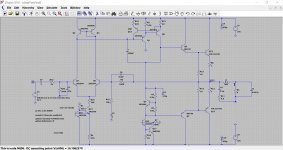
Hi! So i've been hacking away at this circuit for almost a year and it is very close to completion. The first circuit attached (named nobias) was made up by steveu on another thread where he helped me tweak the previous version of this design. I noticed it wasn't stable at 4ohms and also didn't have the greatest voltage output. So I modified it (citing Bob Cordell's Designing Audio Power Amplifiers) and at 16v it gives me the (roughly) 8ohm 15watt or 4ohm 30watt output I am looking for. My questions are:
I would at least like to know if the two sets of transistors above and below the VBE multiplier have the correct resistor-ing? The values dont affect voltage output or frequency response much so i'm assuming its just getting the current as low as possible without affecting output?
How can I get more low end response out of the amplifier? a 60hz cutoff isn't terrible but I would really like to aim for 10 (although it sounds overkill)
Is there anything I should change to make this more stable?
And finally, can I measure total harmonic distortion with spice?
Edit: I don't plan on using 3904's/3906's, they are just for simulation purposes.
Attachments
Last edited:
Q15 has its base and emitter shorted together - you need a current sense resistor between the rail and Q8e/Q15b so that Q15 can act to protect the VAS from over-current.
Q10 and Q13 are upside down (collector/emitters switched). Again a current sensing resistor is missing from the constant current sink.
D6???
C2 very low value, you want it to be reasonably linear down to 20Hz, perhaps 2200µF better choice? Cure the low end cutoff.
C5 is tiny. 22µF would provide better fast switching of drivers.
R10/R11 ???
A couple other thoughts...
DC Offset is 174mV. The mismatch between R20 and R9 is driving this.
Doesn't look like the bias has been set.
Seems odd to use a active current source for the VAS and a simple resistive source for the LTP.
R2 looks high - try 1k or 2k. As Mark pointed out, the emitter of Q15 needs a resistor - try 2k. I believe you will want a degeneration resistor for the emitter of Q8 as well if you're going to use current limiter Q15. Maybe something around 47r or 68r
R8 & R13 seem high. Is this intentional?
The Miller Pole frequency seems high - looks to be close to 4 MHz. I believe most designers keep this around 500kHz.
You're going to the trouble of more complex circuit blocks with the VAS, VAS current limiter and VAS current source, but the input stage is fairly simple. No degeneration resistors, fairly low current, resistor load. Is this intentional?
So heres what I found:
R8 and R13 are a little high just to protect the output devices. Not needed but its there.
removing r10 and r11 make it stop working.
how do I set the bias?
making c2 larger only cuts off frequencies after the 5kish area. I still have the 60hz cutoff problem.
what is the miller pole frequency?
the rest of the advice applied nicely it seems and I even have a little more wattage output.
Do I now have Q8, Q15, Q1, Q13 and Q10 wired correctly now?
Yes the input stage is fairly simple now that you mention it, I assumed Q4 + Q3 was the current source? can this be improved?
Lastly, I assumed R20 just set input impedance, although changing it does affect the amplifier weirdly. should it be the same value as R9?
Attachments
Not for me, but I fixed the broken parts of the circuit first.So heres what I found:
R8 and R13 are a little high just to protect the output devices. Not needed but its there.
removing r10 and r11 make it stop working.
Set input to zero, adjust resistor R5 down till the current in R8/R13 about 50mAhow do I set the bias?
That doesn't make sense to me.making c2 larger only cuts off frequencies after the 5kish area. I still have the 60hz cutoff problem.
Set by the miller capacitor - its complicated, read up on compensation schemes.what is the miller pole frequency?
no, neither has the resistor in the right place. Q8 needs resistor between its emiter and the rail. Same for Q10the rest of the advice applied nicely it seems and I even have a little more wattage output.
Do I now have Q8, Q15, Q1, Q13 and Q10 wired correctly now?
R12 and R20 form a potential divider. R20 should match R9 for balance in the input pair.Yes the input stage is fairly simple now that you mention it, I assumed Q4 + Q3 was the current source? can this be improved?
Lastly, I assumed R20 just set input impedance, although changing it does affect the amplifier weirdly. should it be the same value as R9?
Last edited:
The questions you're asking aren't easy to answer in space of a forum. People have literally written entire books on them. I suggest Douglas Self or Bob Cordell's books on amplifier design. They're pricey but worth it. Rod Elliot's website is also a tremendous (and free) resource.
You may be better off starting with a known and proven design and tweaking it to put your own signature on it. Douglas Self's "Blameless" designs are good if you favor low distortion transparent designs. Rod Elliot's P3A is good if you like some color to your sound. It's also a simple design with a proven pcb available.
Regarding your questions on setting bias and analyzing THD, I encourage you once again to read Mooly's thread. I covers all these questions and more.
You look to be running a 16ma VAS current. This seems very high for a low voltage single output pair amp. I would expect this to be something close to 5ma. If you stick with 16ma, you'll need to ensure the device you choose can handle the heat dissipation.
Your gain and phase margin look OK.
The 100k Input and NFB resistors are high. Most designers choose something around 20k or 30k. This higher value will make life easier for the source driving it, but at the expense of increased Johnson noise.
The 2200u for NFB cap C2 is unnecessarily large. With your 10k R16, you'd only need 10u to achieve a 1.6Hz pole. If you update your R9 / R16 to a more reasonable 20k / 2k then C2 can probably be 47u. As C2 gets larger, PCB layout can be an issue due to physical size.
On a similar note, input cap C7 is too large for your 100k R20. You could drop this to 1u and still have a 1.6Hz pole. If you update R20 to 20k, you can still drop C7 to 4.7u and achieve a 1.7Hz pole.
Your Cdom pole frequency has issues. With the 47p you used, the -3db point is 4.6 MHz with a large hump. I suspect this would lead to stability issue (though I'm far from an expert here). To tame this, you'd need something like 470p.
Other thoughts: You don't have actual VAS or Output devices in your model. It's hard to come to any real conclusions without a these. Many on this forum use the models Bob Cordell has developed. You may want to give these a try.
You'll also want to do some additional analysis in simulation:
Getting this "right" in simulation is the easy part. Then comes layout / PCB design and component choices which is likely to be more challenging.
Once a prototype is available, you'll likely need a scope to check for stability issues. And you'll probably want to repeat some of the simulation analysis in "real-life" on the prototype - simulations don't always hold up in reality. Equipment to test distortion would also be a nice to have.
Not trying to discourage you - just pointing out the road ahead. Taking a know stable design and tweaking it or designing your own PCB for it to accommodate different device choices would be simpler path.
- Noise Analysis
- AC Frequency response
- Square Wave testing
- PSSR testing - add some ripple and noise to the supplies
- Slew Rate
- THD analysis at different frequencies and power levels
- Bias stability - vary supply voltage to determine if bias levels are stable with fluctuating voltage (from mains fluctuations or transformer regulation)
- Review dissipation in devices to ensure operation within SOA
- Open Loop Gain analysis to assess Gain Margin and Phase Margin. Including loop gain review to check for excessive NFB that may lead to instability.
- Probably many others I can't think of at the moment
Getting this "right" in simulation is the easy part. Then comes layout / PCB design and component choices which is likely to be more challenging.
Once a prototype is available, you'll likely need a scope to check for stability issues. And you'll probably want to repeat some of the simulation analysis in "real-life" on the prototype - simulations don't always hold up in reality. Equipment to test distortion would also be a nice to have.
Not trying to discourage you - just pointing out the road ahead. Taking a know stable design and tweaking it or designing your own PCB for it to accommodate different device choices would be simpler path.
You may want to stick with the EF2 output stage or consider CFP. I understand that EF3 can produce superior results, but can be harder to stabilize. Also, I don't think there's much advantage to a EF3s OPS for a low output single pair setup. For a low output design, you may want to consider a CFP output stage. Many people prefer this when only a single output pair is used.
This is a really great attempt actually. I through some different models into the sim and gave it whirl... its... different. Very good in parts ")
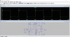
The driver dissipation is relatively high at idle, more than the output devices but so what. It works well.
The only real concerns are the stability, and here it seemed easy to provoke oscillation. The usual Zobel and output inductor did little to help (surprisingly) and a tweak of the compensation was needed. Running the amp at such a low gain is one of the contributory factors... but it can be worked around.
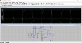
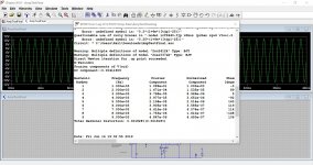
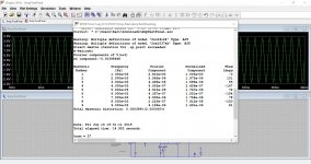
Distortion is shown at 1 watt and 15 watts into 4 ohm. Pretty good.
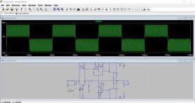
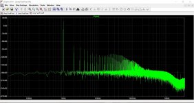
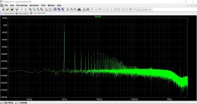
Squarewave testing was where things came undone a little initially as can be seen by the small added capacitive loading.
The driver dissipation is relatively high at idle, more than the output devices but so what. It works well.
The only real concerns are the stability, and here it seemed easy to provoke oscillation. The usual Zobel and output inductor did little to help (surprisingly) and a tweak of the compensation was needed. Running the amp at such a low gain is one of the contributory factors... but it can be worked around.
Distortion is shown at 1 watt and 15 watts into 4 ohm. Pretty good.
Squarewave testing was where things came undone a little initially as can be seen by the small added capacitive loading.
Attachments
I would add when I tinkered with it, reducing the VAS current seem to help with stability issues.
Excellent point on the overall gain. Forgot to mention that. The high NFB factor can cause problems. Perhaps its better to reduce this and then reduce the supply rails to arrive at the same output goal?
Excellent point on the overall gain. Forgot to mention that. The high NFB factor can cause problems. Perhaps its better to reduce this and then reduce the supply rails to arrive at the same output goal?
- Status
- This old topic is closed. If you want to reopen this topic, contact a moderator using the "Report Post" button.
- Home
- Amplifiers
- Solid State
- transistor amplifier design finalization