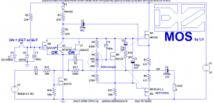
This amplifier is terminally simple, cheap and forgiving, but it remains capable of amplifying in the seventies style: it would have been capable of meeting some HiFi standards of the time.
Of course, nowadays a THD of 0.5% and a full-power bandwidth of 50kHz is only tolerable in audiophile or tube amps, but even compared to a chipamp, it remains easy and accessible.
The design came to birth as a by-product (understand reject) of a request from Daniel: he asked me to design a discrete amplifier that could match a chipamp in performance, simplicity and ease of construction.
I examined a number of options, and I rejected this one because of its inverting design and its (relatively) low performances: in its best implementation, it manages 0.1% THD and 100kHz power bandwidth.
It is nevertheless a neat and effective amplifier, and importantly, it is highly evolutive: this is the plain vanilla version, but serious improvements are possible without too many complications; more on that later.
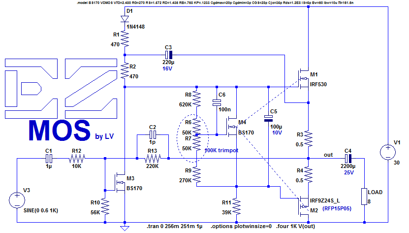
The main drawback of ultra-simple MOS-followers based amps is their output voltage swing heavily curtailed by the MOS threshold voltage, typically several volts under load.
Add the inevitable losses from the source resistors and the drivers and you are left with an output of Vrail minus 5 to 10V for each rail.
For high-power amps, the loss is relatively benign, but with 10 or 15V of total supply voltage, practically nothing is left to drive the load.
EZ-MOS solves the problem by bootstrapping for the positive rail and a "bias memory cap" for the negative one (or GND for a simple amplifier like this one).
The result is a 3-transistor + bias topology capable of swinging 28.5Vpp with a 31V supply: not bad for a simple follower-based amp.
One of the main drawback is the inverting configuration, but even renowned designers like Renardson use it.
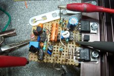
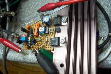
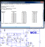
Here are pics of my prototype:
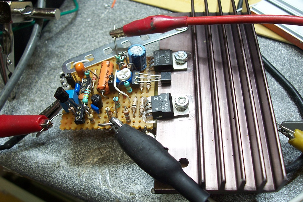

The low-power MOSfets can be almost any low-power type like 2N7000, and the OP can be any approximate complementary vertical pair.
My prototype is wired for a ~30V supply and is capable of putting out ~12W @ 8Ω, but other voltages and load impedances are possible just by scaling R13.
You can probably notice that the board is heavily populated compared to the schematic: that's because of the evolutive aspect.
The prototype includes all the options, but here the jumpers are in the "plain vanilla" position.
More will follow
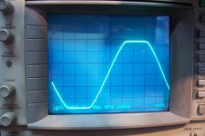
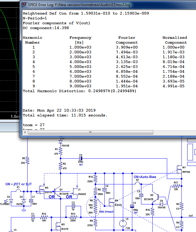
Here is the 10kHz, large signal squarewave response:
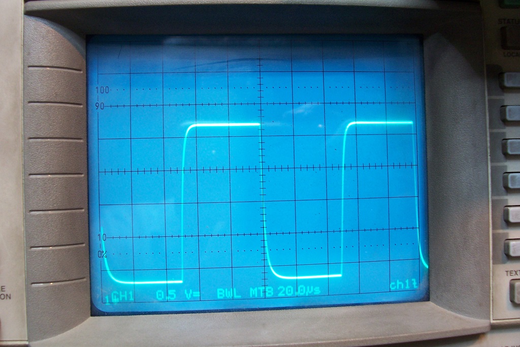
Not blindingly fast for this version obviously, but clean and sufficient for audio purposes, at least in principle.
The simulated THD is a shade over 0.5%; in the same conditions, the measured THD is a shade under 0.5%, thus very close, which is normal for "high" THD levels.
Of course, nowadays a THD of 0.5% and a full-power bandwidth of 50kHz is only tolerable in audiophile or tube amps, but even compared to a chipamp, it remains easy and accessible.
The design came to birth as a by-product (understand reject) of a request from Daniel: he asked me to design a discrete amplifier that could match a chipamp in performance, simplicity and ease of construction.
I examined a number of options, and I rejected this one because of its inverting design and its (relatively) low performances: in its best implementation, it manages 0.1% THD and 100kHz power bandwidth.
It is nevertheless a neat and effective amplifier, and importantly, it is highly evolutive: this is the plain vanilla version, but serious improvements are possible without too many complications; more on that later.
The main drawback of ultra-simple MOS-followers based amps is their output voltage swing heavily curtailed by the MOS threshold voltage, typically several volts under load.
Add the inevitable losses from the source resistors and the drivers and you are left with an output of Vrail minus 5 to 10V for each rail.
For high-power amps, the loss is relatively benign, but with 10 or 15V of total supply voltage, practically nothing is left to drive the load.
EZ-MOS solves the problem by bootstrapping for the positive rail and a "bias memory cap" for the negative one (or GND for a simple amplifier like this one).
The result is a 3-transistor + bias topology capable of swinging 28.5Vpp with a 31V supply: not bad for a simple follower-based amp.
One of the main drawback is the inverting configuration, but even renowned designers like Renardson use it.
Here are pics of my prototype:
The low-power MOSfets can be almost any low-power type like 2N7000, and the OP can be any approximate complementary vertical pair.
My prototype is wired for a ~30V supply and is capable of putting out ~12W @ 8Ω, but other voltages and load impedances are possible just by scaling R13.
You can probably notice that the board is heavily populated compared to the schematic: that's because of the evolutive aspect.
The prototype includes all the options, but here the jumpers are in the "plain vanilla" position.
More will follow
Here is the 10kHz, large signal squarewave response:
Not blindingly fast for this version obviously, but clean and sufficient for audio purposes, at least in principle.
The simulated THD is a shade over 0.5%; in the same conditions, the measured THD is a shade under 0.5%, thus very close, which is normal for "high" THD levels.
Attachments


Ahhh...my kind of experimental DIY ") I like it, whether it is 0.01, 0.1 or even 1% THD but the question is, what would be the approximate or typical ratio of harmonics in the distortion in this design and as you follow through to other implementations? This feature is really significant among popular old designs and also to what we do now, because it determines whether we can live with small amounts of distortion or not. That makes it a good predictor of popularity for the longer term.
I like it, whether it is 0.01, 0.1 or even 1% THD but the question is, what would be the approximate or typical ratio of harmonics in the distortion in this design and as you follow through to other implementations? This feature is really significant among popular old designs and also to what we do now, because it determines whether we can live with small amounts of distortion or not. That makes it a good predictor of popularity for the longer term.
I like it, whether it is 0.01, 0.1 or even 1% THD but the question is, what would be the approximate or typical ratio of harmonics in the distortion in this design and as you follow through to other implementations? This feature is really significant among popular old designs and also to what we do now, because it determines whether we can live with small amounts of distortion or not. That makes it a good predictor of popularity for the longer term.I suspect D1 tries to prevent C3 from pushing current into the +30V top supply rail on a high amplitude peak. With D1 in place the charge on the "top plate" of C3 can be leaked away through a relatively high resistance (>30K) path that ends in R11. Without D1 it can be leaked away through only 470 ohms (R1).
Thanks!Looks good! Nice work
Not really: this is a simple, low power design and anyway with the VAS being also the input stage, moving the input reference from the negative rail to anywhere else would be seriously complicated without adding a transistor (the negative rail would need to be spotlessly clean, which is not practical).Elvee, that looks very simple and interesting!
Any plans for symmetrical +/- rails, to get rid of the output cap?
That said, adding a transistor in the seventies style would be perfectly possible, but this would become another amplifier.
I may discuss it later
Just about anything being of sufficient size and vaguely complementary: IRF240/9240, IRF540/9540, IRF530/9530, and many others. Note that you could mix families: IRF530/IRF9540 for example. If you do so, preferably use the P one as the strongest member because of inherent technological limitations, although the opposite will work anyway, because the circuit is highly tolerant.Also, what other output devices can be used?
If the bias adjustment range becomes insufficient, you can swap the 100K trimpot for a 220K one.
About the bias, 200~250mA is a good trade-of between heat and low-level linearity, but you are free to chose different values
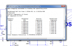
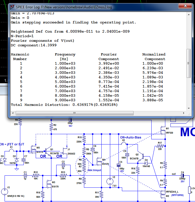
Here is a THD typical profile for this family of amplifiers:Ahhh...my kind of experimental DIY
Because of the non-symetrical topology and the low feedback, low-order, even harmonics tend to be dominant.
Here is the THD residue (0.15%) together with the output signal:
D1 has two roles under large signal conditions:Great. What's D1 for?
When the potential on the positive armature of C3 exceeds the +rail, it prevents its discharge through R1, thus reducing the rms current through this resistor and the subsequent heating, and it also allows C3 to charge at a higher voltage than the normal Vs/4 value, allowing a larger bias current through the VAS and the bias spreader.
Of course, MOSfets don't require a base current, but they need some capacitive current under high slewrate conditions, and this little trick helps a little.
This "dynamic bias" feature can be tweaked by changing the ratio of R1 to R2 (or it can be eliminated if you don't like it)
Under
Both are equally (un)important, and you have a lot of room for manoeuver, see remarks above.i like that i see Elvee .
which is the most important ?, the irf530 or the rfp15p05?
it is a mandatory choice or there is room for maneuver in the choice of output transistors?
--------------------
The first and most obvious upgrade to the base circuit is to add a cascode stage: because of the inverting topology, R12 and its dependent resistors R10 and R13 need to be reasonably large; combined with the largish MOS capacitances, this results in a strong Miller effect.
This effect self-compensates the amplifier, but it is much larger than necessary, resulting in poor dynamic performances.
The solution is extremely simple: add a properly biased device in M3's drain.
The device can be a MOS, BJT or jFET.
A MOS works, but due to its finite transconductance and parasitic capacitances, it adds unwanted poles to the loop, resulting in instability.
The cure is easy: to add a capacitor between its drain and the input, but it kind of negates the usefulness of the cascode.
BJT's or jFETs do not require anything to work properly, but the Idss/Vto of jFETs varies widely, even for a given type, and this could require bias adjustments.
For these reasons, I recommend using a simple BJT: it is completely predictable and the bias source is an ordinary red LED.
With the same LED, a FET like the 2SK125 also works. Some high Idss types could work with no bias at all.
A good point worth noting: the addition of the cascode does not reduce the output swing.
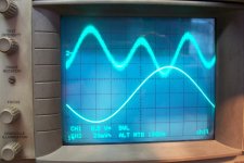
Here is the circuit configured for a BJT cascode:
And here is the same 10kHz squarewave (note the improvement):
Here is the clipping behavior:
--------------------------
Another addition to the base circuit is the RC network C8/R14: it probably looks intriguing.
Its effect is to reduce the THD, from 0.4% to less than 0.15% (in the real circuit), about 10dB.
How does work?
Well, that is not entirely clear at the moment, even for me, and I still need to think about it.
I think it operates through two mechanisms: it somewhat compensates for the distortion the bootstrap reinjects at the input of the MOS (the bootstrap cap is tied to the source of the NMOS, and that's where it should be) and it forces a local degeneration of the OP's by changing the pure input current drive to a ~voltage drive, making the degeneration by the source resistors possible.
It is unexpected though that a local degeneration (reducing the overall loop gain) manages to reduce the global non-linearities: the general rule is exactly the opposite (which does not mean that local degeneration is useless, I hurry to say).
The effect is not an artifact, it has been confirmed in other simulations (this one does not show it, because I used models "similar" to the real circuit, but I include another one, less faithful but in fact more accurate), and in the real world.
If someone has an illumination, please share it....
Now, prepare yourself and fasten your seat-belts, because the next installment will take you to the other side of the quiescent current auto-bias mirror, and its simplicity will match that of the amplifier (1 transistor)!
Attachments

Hi Elvee, I'd like to share a bit of experience. I built a mini F5 clone with IRF 530/9630 in 2014 with bipolar 12V supply without any source resistor on the mosfets. The circuit was thermally stable biased at ~ 450mA. I think you can also reduce the source resistor to < 0.11 ohm or even omit them altogether to gain the advantage of lower H3 and H5.
Thanks for your constructive remarks.
We have to remember that the F5 and EZmos are two very different amplifiers:
The F5 has a common-source output topology, and operates in class A, if I am not mistaken.
EZmos has a more traditional follower OP, and is primarily intended for class AB work (nothing prevents you from increasing the bias to pure class A, but that was not my initial goal).
In principle, one should compare apples to apples, or in this case prevent ourselves from applying apple recipes to oranges.
Despite these caveats, your remarks remain broadly applicable to this amplifier: it would be possible to operate with lower, or even no source resistors at all.
MOSfets, even vertical ones have some in-built compliance, unlike BJT's (under some peculiar circumstances, even BJT's can work without resistors, but that's not something I recommend to beginners or the faint of heart).
Increasing the quiescent current to 450mA would be beneficial: I have observed that the linearity improves with increasing current (in sims, there is a sweet spot at an intermediate value, but not in reality).
A reduction of the source resistors should bring apparent advantages: reduced output impedance, increased damping factor, larger output under load (here, the difference between the 28.5Vpp output and the 31V supply is mostly wasted in the resistors).
Another effect is that it unmasks the true nature of the OP devices: N- and P-MOS are fundamentally different, even when you try to match them better by using a IRF530 and a IRF9630 instead of a 9530.
Asymmetries result in the dominance of even harmonics over odd ones, and in a low-feedback amplifier such as this one, the effect remains present in the output signal.
With source resistors, the characteristics of the two initially dissimilar MOS is evened, allowing non-linearity compensation.
This compensation allows a reduction in the overall THD figure, but it will do so by eliminating the even harmonics, so cherished by some (don't count me in).
To summarize:
Eliminating the source resistors and increasing the bias current will improve the global linearity and favor H2 H4 against H3 H5, but I strongly advise against it:
This amplifier is a beginner's project, and to apply these measures without too many risks requires minimal competences to achieve a good thermal contact between the transistors and the heatsink.
An amateurish attachment might be enough to sustain the permanent 5 ~ 7W caused by the quiescent current, but as soon as a "thermal event" caused by the program contents and the load occurs, it will drive the amp into a fast and irrecoverable thermal runaway.
With reasonably sized resistors, this risk is mitigated.
There is a safer solution for those wanting to alter the THD profile: simply use dissimilar source resistor, for example 0 for one or 0.5 for the other.
It will have a similar effect, but without the risks associated with no resistor at all.
You could use the 0.5 one for the P side, to reinforce its "weakness", or for the N side, to get more subtle effects.
-------------------------
Now, let us examine the quiescent current servo:
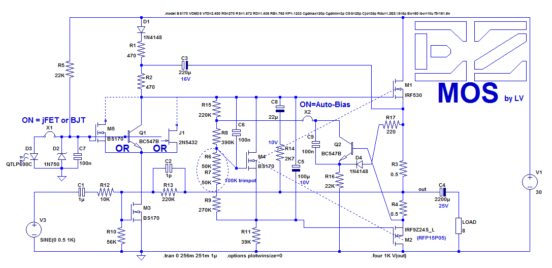
It is built around Q2 and D4: D4 and the B-E junction of Q2 form a kind of diode gate, but with simplified idealized diodes, no current could ever flow into Q2's base: D4's anode is always at a more positive potential than Q2's base.
Actual semiconductor junctions have an exponential behavior though, and R17 in series with D4 also helps shifting the level.
The result is a "sampling gate" that conducts for each minimum of the total voltage across R3 and R4, ie. the zero-crossing of the output current waveform.
This means that the conduction of Q2 will be modulated by how low the cross-conduction (or quiescent) current is.
The collector current is integrated by C9 and alters the conduction of the bias spreader M4 via a resistive divider.
In short, the system imposes a minimal current through the output stage.
Because the amplifier is AC-coupled, the quiescent current is updated at least a few tens of time per second (or continuously under no-signal conditions).
The bias voltage is integrated and held with a time constant of several seconds by C5.
Note that since the circuit does not operate in real-time, it does not allow non-switching operation, unlike the Circlophone for example.
To make the auto-bias active, the bias trimpot is set to zero, and X2 is inserted, allowing the AB-circuit to take control.
The circuit has a very low loop gain, meaning the target current value can still be adjusted with the trimmer.
Alternatively, R9 could be made fixed and larger, and the current could be set by varying R17.
I said earlier that the circuit was not perfect: with this arrangement, the dynamic quiescent current varies between quiescent and large signal conditions.
The peak base current in Q2 increases under large signal, but not enough to compensate the reduced duty cycle, resulting in a lower average current.
That is caused by the inverse exponential behavior of the diode gate.
For example, if the static current is set to 250mA, the dynamic large signal current is reduced to ~175mA.
I prefer to see that as a "feature", not a negative: it increases the first-watt, pure class A operation range and equalizes the heat output for different conditions.
In fact, my first implementation of the circuit largely compensated the variation, but in the end I opted for this one.
The first version had the diode in the base instead of the emitter, and the bias resistor R16 was tied to the positive armature of C3; this made the average bias current dependent on the signal level, and could be made to compensate the reduction caused by the dynamic operation.
In the end, I opted for this version, also because it gives Q2 one more Vbe of working room, increasing the range of correction possible.
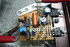
Here is a pic of the circuit with the AB active (not much has changed):

We have to remember that the F5 and EZmos are two very different amplifiers:
The F5 has a common-source output topology, and operates in class A, if I am not mistaken.
EZmos has a more traditional follower OP, and is primarily intended for class AB work (nothing prevents you from increasing the bias to pure class A, but that was not my initial goal).
In principle, one should compare apples to apples, or in this case prevent ourselves from applying apple recipes to oranges.
Despite these caveats, your remarks remain broadly applicable to this amplifier: it would be possible to operate with lower, or even no source resistors at all.
MOSfets, even vertical ones have some in-built compliance, unlike BJT's (under some peculiar circumstances, even BJT's can work without resistors, but that's not something I recommend to beginners or the faint of heart).
Increasing the quiescent current to 450mA would be beneficial: I have observed that the linearity improves with increasing current (in sims, there is a sweet spot at an intermediate value, but not in reality).
A reduction of the source resistors should bring apparent advantages: reduced output impedance, increased damping factor, larger output under load (here, the difference between the 28.5Vpp output and the 31V supply is mostly wasted in the resistors).
Another effect is that it unmasks the true nature of the OP devices: N- and P-MOS are fundamentally different, even when you try to match them better by using a IRF530 and a IRF9630 instead of a 9530.
Asymmetries result in the dominance of even harmonics over odd ones, and in a low-feedback amplifier such as this one, the effect remains present in the output signal.
With source resistors, the characteristics of the two initially dissimilar MOS is evened, allowing non-linearity compensation.
This compensation allows a reduction in the overall THD figure, but it will do so by eliminating the even harmonics, so cherished by some (don't count me in).
To summarize:
Eliminating the source resistors and increasing the bias current will improve the global linearity and favor H2 H4 against H3 H5, but I strongly advise against it:
This amplifier is a beginner's project, and to apply these measures without too many risks requires minimal competences to achieve a good thermal contact between the transistors and the heatsink.
An amateurish attachment might be enough to sustain the permanent 5 ~ 7W caused by the quiescent current, but as soon as a "thermal event" caused by the program contents and the load occurs, it will drive the amp into a fast and irrecoverable thermal runaway.
With reasonably sized resistors, this risk is mitigated.
There is a safer solution for those wanting to alter the THD profile: simply use dissimilar source resistor, for example 0 for one or 0.5 for the other.
It will have a similar effect, but without the risks associated with no resistor at all.
You could use the 0.5 one for the P side, to reinforce its "weakness", or for the N side, to get more subtle effects.
-------------------------
Now, let us examine the quiescent current servo:
It is built around Q2 and D4: D4 and the B-E junction of Q2 form a kind of diode gate, but with simplified idealized diodes, no current could ever flow into Q2's base: D4's anode is always at a more positive potential than Q2's base.
Actual semiconductor junctions have an exponential behavior though, and R17 in series with D4 also helps shifting the level.
The result is a "sampling gate" that conducts for each minimum of the total voltage across R3 and R4, ie. the zero-crossing of the output current waveform.
This means that the conduction of Q2 will be modulated by how low the cross-conduction (or quiescent) current is.
The collector current is integrated by C9 and alters the conduction of the bias spreader M4 via a resistive divider.
In short, the system imposes a minimal current through the output stage.
Because the amplifier is AC-coupled, the quiescent current is updated at least a few tens of time per second (or continuously under no-signal conditions).
The bias voltage is integrated and held with a time constant of several seconds by C5.
Note that since the circuit does not operate in real-time, it does not allow non-switching operation, unlike the Circlophone for example.
To make the auto-bias active, the bias trimpot is set to zero, and X2 is inserted, allowing the AB-circuit to take control.
The circuit has a very low loop gain, meaning the target current value can still be adjusted with the trimmer.
Alternatively, R9 could be made fixed and larger, and the current could be set by varying R17.
I said earlier that the circuit was not perfect: with this arrangement, the dynamic quiescent current varies between quiescent and large signal conditions.
The peak base current in Q2 increases under large signal, but not enough to compensate the reduced duty cycle, resulting in a lower average current.
That is caused by the inverse exponential behavior of the diode gate.
For example, if the static current is set to 250mA, the dynamic large signal current is reduced to ~175mA.
I prefer to see that as a "feature", not a negative: it increases the first-watt, pure class A operation range and equalizes the heat output for different conditions.
In fact, my first implementation of the circuit largely compensated the variation, but in the end I opted for this one.
The first version had the diode in the base instead of the emitter, and the bias resistor R16 was tied to the positive armature of C3; this made the average bias current dependent on the signal level, and could be made to compensate the reduction caused by the dynamic operation.
In the end, I opted for this version, also because it gives Q2 one more Vbe of working room, increasing the range of correction possible.
Here is a pic of the circuit with the AB active (not much has changed):
Attachments

I think the IRF530/RFP15P05 are good, but not advisable for the larger verticals. I had thermal runaway with parts of higher Gm such as the IRF 540/9540, 640/9640 and the IRFP 240/9240 at fix bias without source resistors nor thermal feedback, from very low quiscent like 30mA onwards.... it would be possible to operate with lower, or even no source resistors at all.
MOSfets, even vertical ones have some in-built compliance, ...
Off course your opinions are correct regarding the risk, but I feel that 0.5 ohm is a bit excessive, the H3 has riisen above -60dB at 1W.
Last edited:
To illustrate what I said about the source resistors, here are a few sim examples, @1W & 100mA fixed bias.
First the circuit with its 0.5Ω source resistors:
The THD is 0.25% with a moderate dominance of H2 H4 (in the same conditions, the measured value on the real circuit is 0.085%).
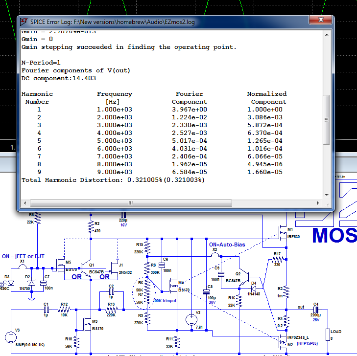
Now, same conditions but 0.1Ω resistors:
The THD has had a huge increase, to 0.63%, and now H2 and H4 are heavily dominant.
If the 0.2Ω is placed in the NMOS, with the other defaulted to 1mΩ, the THD level and the even character is even more apparent:
With the opposite situation, the THD has been reduced, almost to the original value, but still with a strong even character:
All this shows that it is perfectly possible to tweak/manipulate the harmonic profile without thermal risks or a penalty in the global THD
First the circuit with its 0.5Ω source resistors:
The THD is 0.25% with a moderate dominance of H2 H4 (in the same conditions, the measured value on the real circuit is 0.085%).
Now, same conditions but 0.1Ω resistors:
The THD has had a huge increase, to 0.63%, and now H2 and H4 are heavily dominant.
If the 0.2Ω is placed in the NMOS, with the other defaulted to 1mΩ, the THD level and the even character is even more apparent:
With the opposite situation, the THD has been reduced, almost to the original value, but still with a strong even character:
All this shows that it is perfectly possible to tweak/manipulate the harmonic profile without thermal risks or a penalty in the global THD
Attachments


What happens if R3, R4 both at 0.5 and a diode parallel with R4?...With the opposite situation, the THD has been reduced, almost to the original value, but still with a strong even character...
It slightly reduces the overall THD level, without greatly affecting the harmonic profile:

In // with R3, it changes even less, but these are sim results and in reality they will heavily depend on the actual MOSfets (remember that the measured THD level is ~1/3rd of that predicted by the sim)
In // with R3, it changes even less, but these are sim results and in reality they will heavily depend on the actual MOSfets (remember that the measured THD level is ~1/3rd of that predicted by the sim)
Attachments
I must have read something backwards. Looks like 0.38 is higher than 0.25, from earlier? But, it is like your 3rd example with the 1m vs 0.2 resistors, except different than all of the examples in what happens to the bass beat if the popular double-woofer speakers were connected. MiniStatementsIt slightly reduces the overall THD level, without greatly affecting the harmonic profile...
A different option is the one diode across both of the resistors. I'm not sure if that's safe? But, what happens is that the 0.5 resistors change to 0.25 dynamically, per the bass beat.
Maybe a diode per each is better with asymmetric music signal? Some of this might allow values approaching 1R, if that would be helpful with the THD? Although if the resistor value were too high then the diode switching might be noise. I have no idea.
Just something to consider.
I had forgotten that the examples above were based on 1W/8ohm.
With such a low current, even schottky's would not be able to begin conducting and change the behavior
With the diode, I increased the power to ~12W, near the maximum, which explains the THD increase to 0.46%.
By increasing the resistors to much more than 0.5, it would be possible to lower the action threshold, but with an effect so brutal and severe, it would resemble an instrument amp + effect box
If I use a $9, 24v 96W (36W clean) SMPS, then the diode idea isn't needed because it doesn't switch on (thus also measuring that the 0.5 resistors are perfect).
That's probably 8W to 8R size; but, the laptop style power supply is convenient.
I'd wonder about a ~2db soft clipper, with engagement set to when the amp has started clipping (just a clip-duration reduction scheme). Seems another useful tube amp like feature. I wonder what the options are for that?
UK studies fets first at uni, so in a few months when the rains and studies start, there could be some more of these amplifiers made. If 24v power, EZmos is right sized for office, dorm, kitchen and bedroom.
Good application matching! Just a few fets makes a power amp for most common source in most common room size and using SMPS laptop pack. The aspects match up to a good combination of doable and useful.
That's probably 8W to 8R size; but, the laptop style power supply is convenient.
I'd wonder about a ~2db soft clipper, with engagement set to when the amp has started clipping (just a clip-duration reduction scheme). Seems another useful tube amp like feature. I wonder what the options are for that?
UK studies fets first at uni, so in a few months when the rains and studies start, there could be some more of these amplifiers made. If 24v power, EZmos is right sized for office, dorm, kitchen and bedroom.
That's a good feature! The singleton-input inverting amp matches well with modern headphone sources (laptop, chromecast-audio, bluetooth, digi-tuner, phone) and they've got digital volume control already....remember that the measured THD level is ~1/3rd of that predicted by the sim...
Good application matching! Just a few fets makes a power amp for most common source in most common room size and using SMPS laptop pack. The aspects match up to a good combination of doable and useful.
I do not like very much "artificial" soft clippers, because they inevitably reduce the max undistorted output power.I'd wonder about a ~2db soft clipper, with engagement set to when the amp has started clipping (just a clip-duration reduction scheme). Seems another useful tube amp like feature. I wonder what the options are for that?
When the behavior is natural, as for tube amps, this is certainly a bonus, but otherwise I don't think so.
A fast and relatively transparent anti-clipping agc/compressor Peavey-style is certainly preferable, but it would make the circuit much more complicated if implemented with discretes.
I will think about it anyway.
That early engagement problem is avoided by: hard/brink engagement with soft/minimal effectiveness (1 or 2 db at most). In other words 'soften' the opposite parameter. Good function is preventing a clip from being louder than max undistorted output. Other possible functions are (fast recovery) decrease duration of clip (nip off the corners to decrease flat top span/duration), or clip anything other than the outputs (any smaller discharge).I do not like very much "artificial" soft clippers, because they inevitably reduce the max undistorted output power....
Both large and small amplifiers need means that doesn't involve increased power voltage.
Found one. Last schematic on the Tracerphone thread. I had it set slightly too strong. I used it with a little tuner and speaker, so I it was set to resist those loud CAR commercials and caffeinated DJ's. Not very much speaker amp, but I bet the huge imaging would make it highly addictive as a line or headphone amp....A fast and relatively transparent anti-clipping agc/compressor Peavey-style is certainly preferable, but it would make the circuit much more complicated if implemented with discretes....
Last edited:
- Status
- This old topic is closed. If you want to reopen this topic, contact a moderator using the "Report Post" button.
- Home
- Amplifiers
- Solid State
- Easy-MOS is a simplistic, efficient and evolutive all-MOS amplifier for beginners