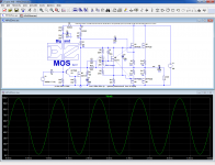
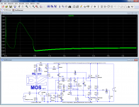
By popular demand, here is a beefed-up version of EZmos: in this example, it can deliver ~150W/8Ω, but other sizes are possible.
The changes required are relatively minor, and they can be applied to any of the versions: cascoded, auto-bias, etc.
Note that like most of the single-supply amplifiers, EZmos will generate a significant power-on thump.
For smaller versions, that is something one can live with, but with 150W output (or more on 4Ω), it is prudent to take preventive measures, like a speaker delay-relay.
I will try to think of smarter solutions, built in the amplifier circuit itself.
Attachments
That really helps.Dear LV & Daniel, My thinking is that +50 Volts DC is convenient, the main capacitors can be 63 Volts rating. The output can be 16 V giving a nice ~30 watts output to 8 ohms. This level of output can be quite adequate for some. SMPSs of 48 Volts rating are available.
If the voltage goes higher, we have to use higher voltage rated Elcos which are not easy to source everywhere. --gannaji
So, 24v to 50v range. A full step.
It does cover two different applications, since power voltage scales in similar proportion to speaker&room sizes--at the higher voltage it works in the living-room, with the TV. That is different than the original application with small room music.
An overly broad range may prevent optimizing component values on the schematic, but the variety can be remedied in your own lab.
However, if going without a lab purchase, you'll need two optimized schematics (at lower and at higher voltage), for covering the range of 24 to 50. A lower voltage schematic exists already. The optimized-at-higher-voltage schematic is missing. I suggest that you should ask for it.
The 50v might not be too convenient. Being mindful of the longevity derating (a third clearance), it looks like 80v cap(s) on the rails, but caps in the amp can be smaller--check with simulator voltage probe (it is the one and only easy to use function of the simulator)....+50 Volts DC is convenient, the main capacitors can be 63 Volts rating...
Fortunately, 63v rail cap does seem workable with up to a 48v power supply.
On my attempt to test this notion, I had tried a 25v rail cap in combination with an adjustable voltage supply and went for some brinkmanship--how far until the subjective quality fell and then turn it back down until the quality is good. Mainly, had I lowered the voltage until the cap didn't resist/strain. That dial is set to 19, with the 25v cap. Multiply power voltage figure by at least 1.32 for the minimum capacitor derating.
That's enough to function for now, but not for later. There was not enough derating for cap wear over time.
If lasting is desirable (such as milspec and/or round-the-clock service), the derating multipler begins at 1.5 (the cap with 1.5x more voltage spec than the supply voltage). Thus, if built to last, the 63v rail cap is usable at up to...Wikipedia: Answer to the Ultimate Question of Life, the Universe, and Everything (42)
By popular demand, here is a beefed-up version of EZmos: in this example, it can deliver ~150W/8Ω, but other sizes are possible.
The changes required are relatively minor, and they can be applied to any of the versions: cascoded, auto-bias, etc.
Note that like most of the single-supply amplifiers, EZmos will generate a significant power-on thump.
For smaller versions, that is something one can live with, but with 150W output (or more on 4Ω), it is prudent to take preventive measures, like a speaker delay-relay.
I will try to think of smarter solutions, built in the amplifier circuit itself.
Awesome!!!!
Yes, a high voltage schematic was needed. Now with 2 points, low and high, it is possible to compare for building different size amplifiers.
For the thumps, even the 150W amplifier could use speakers capable of handling 150W. However, if speakers too small to handle the amp, a protection could sense and switch when the output cap reaches charge. The TDA8932 does that, particularly at pins 19 and 30.
BS. Think rather of simple and lazy, hazy, slightly stupid, summer-friendly solutions!...
I will try to think of smarter solutions, built in the amplifier circuit itself.
...
1. flip the devices and make a P-mos version; and keep the neg. ground. By the virtue of topology, the thump will be minimized.
2. keep the N-mos trannies (as is now) and flip the power; make it "positive gnd". (flip C1, C8, C7, C4 and do something magickal with/around R15). With tweaking of the time-constants you can optimize the turn-on behavior. My lazy estimate is that the thump will be now proportional to the ratio of R11+R1+R2/(R1+R2), perhaps you could do something there as well. And with the high voltage; perhaps you could also delete the flyback D1.
By popular demand, here is a beefed-up version of EZmos: in this example, it can deliver ~150W/8Ω, but other sizes are possible.
The changes required are relatively minor, and they can be applied to any of the versions: cascoded, auto-bias, etc.
Note that like most of the single-supply amplifiers, EZmos will generate a significant power-on thump.
For smaller versions, that is something one can live with, but with 150W output (or more on 4Ω), it is prudent to take preventive measures, like a speaker delay-relay.
I will try to think of smarter solutions, built in the amplifier circuit itself.
Vbe Bs170 can be replaced by irf610? Thanks
These are not stupid solutions: I considered them myself, but I would prefer to keep the conventional topology, negative ground, and everything referred to it (and the NMOS VAS too).BS. Think rather of simple and lazy, hazy, slightly stupid, summer-friendly solutions!
1. flip the devices and make a P-mos version; and keep the neg. ground. By the virtue of topology, the thump will be minimized.
2. keep the N-mos trannies (as is now) and flip the power; make it "positive gnd". (flip C1, C8, C7, C4 and do something magickal with/around R15). With tweaking of the time-constants you can optimize the turn-on behavior. My lazy estimate is that the thump will be now proportional to the ratio of R11+R1+R2/(R1+R2), perhaps you could do something there as well. And with the high voltage; perhaps you could also delete the flyback D1.
I am close to an alternative solution, not absolutely perfect (there might be a volt or two of movement), but terminally simple.
Sure, the gate divider might need to be tweaked, but other than that, there is no obstacle.Vbe Bs170 can be replaced by irf610? Thanks
--------------------------------------------------------------------
One or two more points:
The high power version has not been physically tested: it works in sim, and it is not hugely different from the lower power one, thus the chances it works are good, but you can never be 100% sure until it is built and tested.
All the other versions have been tested, but at 35V supply max.
In the HiPo version, the VAS dissipates almost 3W, and needs a heatsink.
It is probably not necessary to keep such a high quiescent current in the VAS (~50mA), but I prefer to leave everything in the condition for the moment, as a lower current might impact the SR and loop-stability.
Feel free to experiment if you build that version, and report the results: both positive and negative ones are welcome (negatives tend to be more useful for improvements)
LV, any thoughts on the output cap? Does it make distortions (much) worse?
There is another active thread discussing 'coupling capacitors impact on distortion' I've been following, but there is no consensus so far, if output cap impact is measurable, and how significant it is..
Is it something that sim would show?
I guess it won't be trivial to re-design easy-MOS with symmetrical rails?
I have measured the distortion caused by capacitors in this role, and they are orders of magnitude below the intrinsic THD of this design (between 0.2 and 0.002% depending on the variant), so there is nothing to worry about here, unless you think that cap-distortion is particularly nasty and unbearable (which does not seem to be the case).
It is also perfectly possible to include the OP cap in the FB loop, but that is something Daniel explicitly didn't want, and as a result I excluded it from the start.
It could be included, and a dual supply version is also possible, but without the DC accuracy of an input LTP (which Daniel didn't want), it loses much of its sense.
This project complies with a number of specifications (edicted by Daniel), and it implies some design choices.
Some seem very happy with them, others would like to convert the project into something more "modern", more mainstream.....
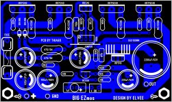
Nice thiagomogi!
Please can you post a black&white for home etching?
An observation on that PCB layout - the feedback path is taken from the wrong place on the output node - it should come from the output capacitor, where the two non-linear currents of the output devices have already been summed. If PCB traces were really zero resistance this wouldn't be an issue, but they have resistance. See slide #69 on this presentation: 1 AES AMSTERDAM 2008 Power Amplifier Workshop. 2 Power amplifier configurations The standard configuration Single differential input stage + push-pull. - ppt download
Neat design, but I was going to give the same advice as Mark:
An observation on that PCB layout - the feedback path is taken from the wrong place on the output node - it should come from the output capacitor, where the two non-linear currents of the output devices have already been summed. If PCB traces were really zero resistance this wouldn't be an issue, but they have resistance. See slide #69 on this presentation: 1 AES AMSTERDAM 2008 Power Amplifier Workshop. 2 Power amplifier configurations The standard configuration Single differential input stage + push-pull. - ppt download
One or two additional suggestions:
-Include an on-board fuse: single supply amps are easy to protect that way, and it is worth including, even if builders chose to strap it instead.
-Include a local bypass cap (not critical, 47µ/160V for example): the design is relatively insensitive to the supply impedance, but if there is a significant wiring length between the main reservoir cap and the amplifier, it will be necessary.
I would also suggest to include all the possible options (cascode and auto-bias) on the board: it will give a maximum of flexibility, and if a builder chooses not to implement one of them, the components can simply be omitted or strapped.
I am currently refining the thump-minimizing network, and implementing it would definitely be worthwhile too.
I am going to prepare a new schematic showing explicitly all of the above.
Nytech had a simple pop-killer that attached to the VAS (or positive output device base/gate in your case). It looked like a cap-multiplier; pnp; and a diode. Usual values 680k/22uf, a BC556 and a 1N4148.
Nytech CA 202 schematic or service manual?
It's easy to spot when you know what to look for.
Nytech CA 202 schematic or service manual?
It's easy to spot when you know what to look for.
The thump-killer circuit is trickier to implement than what I expected: one of the main difficulties resides in the bootstrapping/over-the-rails drive of the MOSFets.
It conflicts with two of the main requirements of such a network:
a) Be totally transparent and inobstrusive after startup
b) Reset to initial conditions when the power is removed
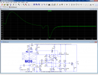
Here is the conventional approach (D3, D4, C9):
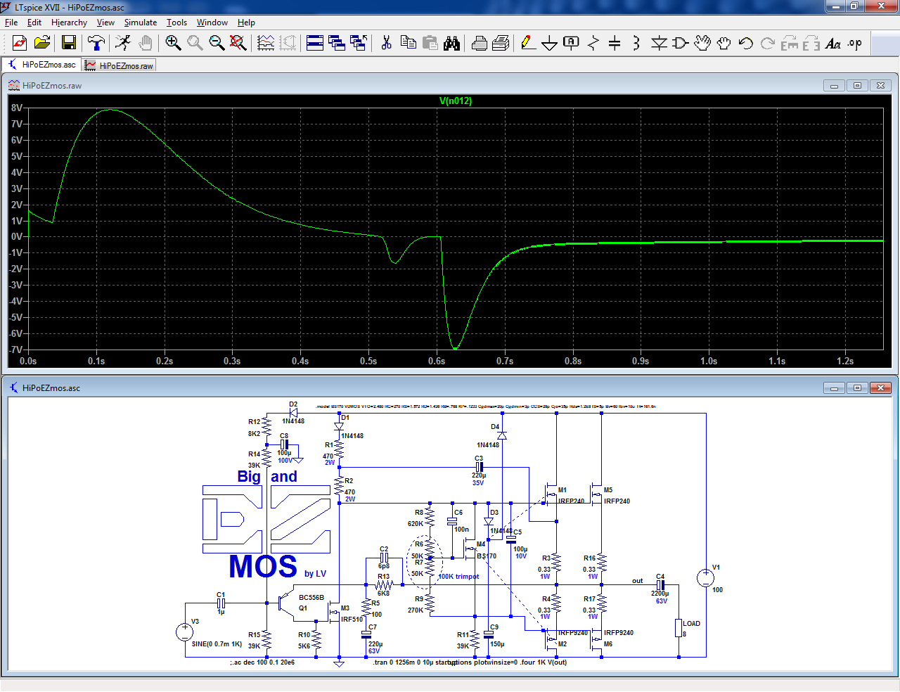
It has a number of issues: a thump and an after-bounce remain (7 to 8V), and D3 and D4 will clip positive excursions.
A zener could be placed in series with D4, but C9 will be left more or less floating, because a leakage resistor to V+ will also cause marginal clipping/distortion.
A more elaborate solution is this circuit: it reduces the amplitude of the thump, and it takes care of all the other issues: bounce, injection of unwanted distorted signal, capacitor reset, etc.
(D3 to 6, C9, 10, R18 to R20)
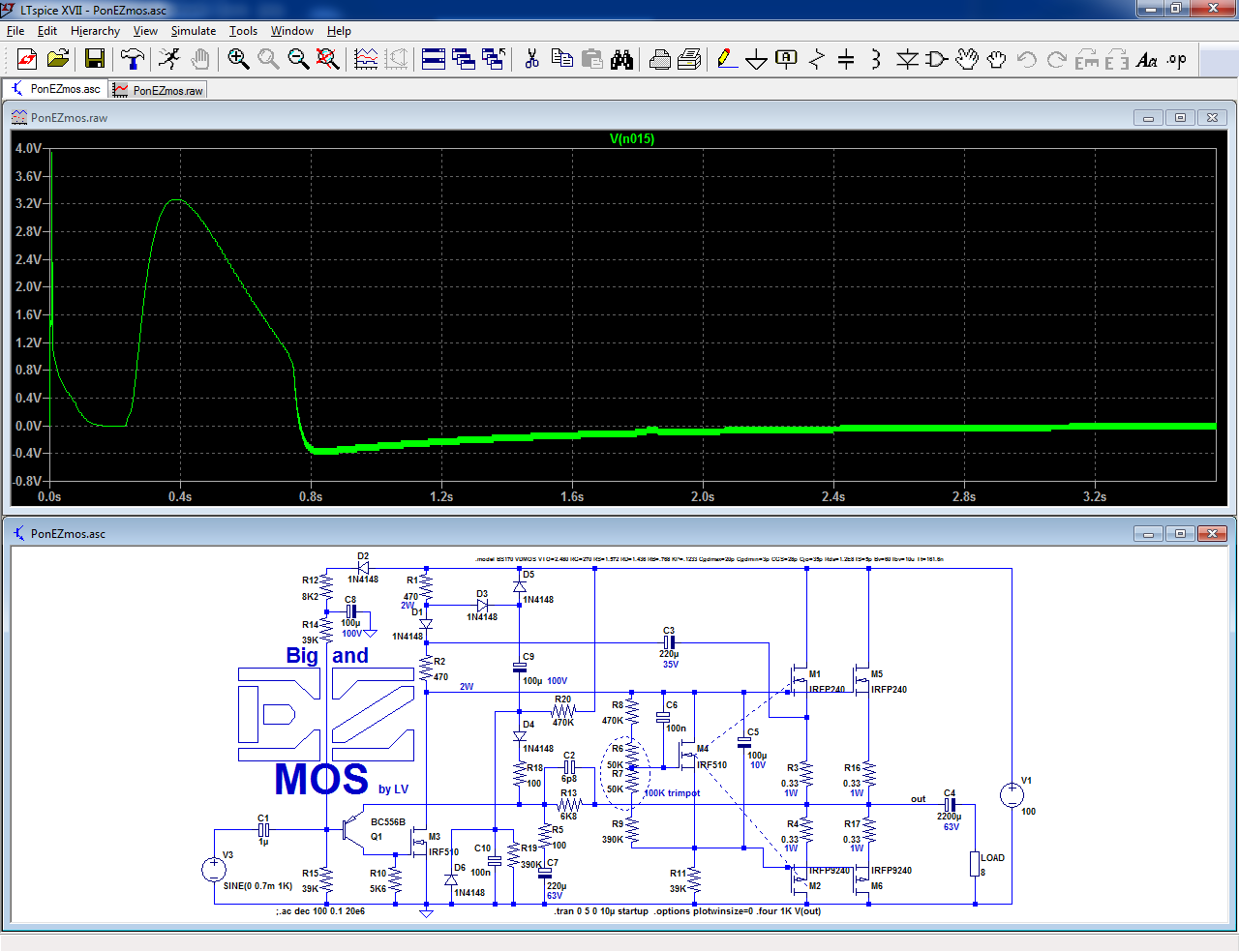
It is rather complicated though (but not expensive).
If someone can spot a weakness or has a better idea, I welcome any comment or criticism.
It conflicts with two of the main requirements of such a network:
a) Be totally transparent and inobstrusive after startup
b) Reset to initial conditions when the power is removed
Here is the conventional approach (D3, D4, C9):
It has a number of issues: a thump and an after-bounce remain (7 to 8V), and D3 and D4 will clip positive excursions.
A zener could be placed in series with D4, but C9 will be left more or less floating, because a leakage resistor to V+ will also cause marginal clipping/distortion.
A more elaborate solution is this circuit: it reduces the amplitude of the thump, and it takes care of all the other issues: bounce, injection of unwanted distorted signal, capacitor reset, etc.
(D3 to 6, C9, 10, R18 to R20)
It is rather complicated though (but not expensive).
If someone can spot a weakness or has a better idea, I welcome any comment or criticism.
Attachments

Yes, if the rise is slow enough, there will be no thump or bounce, but I try to use crude and rude solutions only as a last resort.You could insert a series cap-multiplier with sufficient t-const before the D1 (or also the input bias via D2). Crude and rude. Say, 2sec of slow rise. (Slow ramping instead of clamping; it even rhymes).
We will see what consensus will emerge: we are not in a hurry
New layout, hope this is better. thanks
That is a significant improvement over the previous version.
Some nitpickers might still argue, but that would apply to a ppm-THD capable amplifier, which is not the case here: currently, the THD is around 0.025%, and there is no point in further improvement (for this particular aspect).
I am going to produce a schematic including all the options and improvements, so do not hurry to spend efforts and time on other versions for now, unless members prefer single-purpose PCB's: plain vanilla for this one, cascoded for another one, auto-bias, anti-thump, etc.
I think that a common PCB is the best solution, because some people might already have a speaker relay installed in their frame, others will hate the auto-bias idea, etc: a single PCB design can cover cover any mix of options, with little penalty regarding size or complexity: the amplifier equivalent of a swiss knife.
Thanks for your work and dedication anyway
- Status
- This old topic is closed. If you want to reopen this topic, contact a moderator using the "Report Post" button.
- Home
- Amplifiers
- Solid State
- Easy-MOS is a simplistic, efficient and evolutive all-MOS amplifier for beginners