The balanced to single ended conversion at the input amp in both the Bryston and the clone is very simple and results in different input impedances on the + and - outputs, as well as poor common mode rejection.
Is that referring to the 4B or some other model?
Can you point to what is causing that imbalance?
On the 28B, it's very symmetric throughout, and I don't see anything that could cause an imbalance there..
There is definitely one detail to pay attention to in the 28B, which is at the input before the DOAs, right at the xlr plug, those 2 100ohms resistors should be paired up for best cmrr...
I would pair up as much stuff as possible, even the coupling caps... But if there are caps already on the previous device that feeds the amp, then those caps can just be omitted.
I'm designing for a xover feeding 4 power amps, and for the low end channel, using a 28B module with the balanced input, I plan to put a line driver on that xover channel output, so it'll be balanced all the way, even though the actual link between them will be quite short... I can dispense with those coupling caps.
The 15V rails and component choice are just so I could knock up a quick prototype for proof of concept. I'm designing one "production" version for the Bryston input amp and another for the Bryston power amp. All the methods of taming the undefined vas current with a complementary differential input pairs essentially depend on fixing the voltage at the junction of the ltp and current mirror collectors ( a high impedance point ). The way you've done it in your simulations puts 2Vbe plus a degeneration resistor between the negative rail and the collector junction for both the mirror and the darlington pair. The vas current depends approximately on the ratio of the current mirror and vas degeneration resistors. You need the darlington pair, the 10k resistor R27 and the helper transistor for this to work. You can't set the vas current precisely this way, only good ball park. The olg is reduced by the resistor R27 and the exact value of the vas current depends on the hfe of the input transistors. What I've done is to fix the vas current(s) directly by making the vas part of a current mirror. If you look at my circuit diagram you'll see that the bases of the vas transistors are each joined to the base of an identical, but diode connected, transistor with a degeneration resistor equal to that of the vas. The 2.7k resistor joining the collectors of these diode connected transistors ensures that 10mA flows through each of them. Because the bases of the diode connected transistors are at the same potential as the vas bases then the same current ( 10mA ) must flow through both of them. A classic current mirror. The vas current defined in this way is much more precisely fixed than by the method you used in your simulations, it doesn't slug the input ltp pairs with a differential resistor load, it allows greater freedom of component choice, uses fewer parts, and the vas is naturally current limited. As I showed you previously this technique has been used in several very successful amplifier designs - what's not to like?

As regards the balanced inputs, a single opamp implementation as used in both the Bryston and the clone , looks symmetrical ( but isn't ), and can never be optimal, although it works. Look it up on the web or in Douglas Self's books. You need something like a a three opamp instrumentation style amplifier, or Self's four opamp circuit to get close to optimal. The THAT1200 series of devices has all of this on a single chip as well as a patented method of common mode rejection improvement. Implementing this with discrete opamps, far less discrete components, would be an awful lot of hard work and use a lot of pcb real estate.
Very interesting stuff, and I'll have to do some sims later on. I'm working on something right now, but I'll play with this soon.
I wonder if there will be a real improvement in performance with this. The sims done so far have shown an improvement is possible, and it seems to be working fine. Now we need to compare all this stuff...
I wonder if there will be a real improvement in performance with this. The sims done so far have shown an improvement is possible, and it seems to be working fine. Now we need to compare all this stuff...
I've added a BD139/140 output stage to my design from post #190 and reduced the gain to 2 to make it compatible with the Bryston/Clone input board. Its still unconditionally stable and I can see no difference between the sine/square oscillogarms for an unloaded or 1k output load. I've also designed a THAT1206 balanced input circuit and an improved power supply where the pass transistors don't get anything like as hot as they do with the supplies on the Clone input board. So as far as my take on the Bryston Clone input board is concerned that's me done - design finalised! I could go on and tart up the current sources and current mirrors, as well as other minor improvements, but I think I would be into diminishing returns for what is, after all, only a buffer amp with a bit of gain. Eventually I'll get around to doing a pcb. However, I'm pretty pleased with the way that this has turned out so I've started design work on power amplifier which uses a much more sophisticated version of this topology. I may or may not use a Bryston style output stage - I'll probably build prototypes of both a Bryston and conventional output stage for comparison.
Hi again.
Chalky I have done some work on the bryston amp, I have raised the bias as we talked about, and noise looks better i think, but what's really bugging me is that bad noise figures from 20 to 500 hz, I tried better trafo shielding, twisted wires, shielded signal wire grounded in one end , but I can reduce noice with any of those approaches, maybe you have an idea I haven't tried.
The attached photo is 5.75 volt rms into 8 0hm load.
Amp is now idling at 160 watts in total.
Attachments
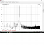
First off is the noise real and not an artefact of the fft? If its real you need to find out where its coming from - the grounding scheme, the input stages, the power stages, or the the power supplies. What about the parallel R and C from signal ground to chassis on the pcbs. Are these in or out? If they are all in you may have made ground loops.
Well I investigated some more today, and you're right, most of the 20 to 500 hz is not from amp, I need some better shielded cable around audio input and the attenuator box, tried touching the 68 of Miller cap, and that immediately lowered noise all over, the Miller cap is a vintage Russian, big and bulky, so couldn't mount it on pcb but on extended legs, think I will have to buy some who fit pcb footprint, in order to get lower noise.
You can get the ATC Semitec E-202 CRD from Rapid Electronics in the UK. Failing that you can use a jfet with an Idss of 2mA ( but watch the voltage ), make up a two terminal constant current source on a small poece of perfboard, or in the last resort use a resistor. Hope that helps.
You can get the ATC Semitec E-202 CRD from Rapid Electronics in the UK. Failing that you can use a jfet with an Idss of 2mA ( but watch the voltage ), make up a two terminal constant current source on a small poece of perfboard, or in the last resort use a resistor. Hope that helps.
Thanks Chalky...will try
You can get the ATC Semitec E-202 CRD from Rapid Electronics in the UK. Failing that you can use a jfet with an Idss of 2mA ( but watch the voltage ), make up a two terminal constant current source on a small poece of perfboard, or in the last resort use a resistor. Hope that helps.
Hi..chalky.....please give me the value of suitable resisters for main board 2 CRD ...that is easy and cheap for me.
You need to let me know what your power supply voltage is going to be before I can calculate the resistor values for you.
Thanks Chalky for your immediate reply.....please give me two values for 55v and 92v. And other thing I want to know is should I use high voltage film/ceramic capacitors other than electrolytes? Thanks
Fetamp you need 11k resistors for a +/-55V supply and 18k for a +/-92V supply. I wouldn't use +/-92V supplies as you'll exceed the Vce of some of the semiconductors. Personally I would regard +/-75 as the absolute maximum.
Thanks a lot Chalky will proceed with your advice....will contact if I need further assistance.
- Home
- Amplifiers
- Solid State
- Bryston 4B SST clone