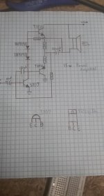
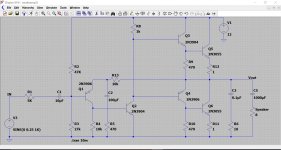
Hi, i've been trying for quite some time to crack the code to designing transistor power amplifiers with little success. I have decided to start with an amplifier with this or similar topology but I cannot seem to get anything to work. My knowledge is very beginner level.
Firstly, can I just connect the speaker to ground?
I am working with TIP31/32 transistors for the drivers and 3707 for the VAS. I am wondering if I need to use different transistors. I am thinking it is an impedance problem, do I need another stage to drive the VAS? I have tried turning the level way up on my signal generator so I can rule the need for another voltage amplifier, but how about a current driver of some sort (1:1 voltage gain) in front of this circuit?
I have also read about a voltage comparator (with a current driver transistor) type stage for the feedback loop to drive VAS, how would I go about designing this?
I understand the power output/efficiency is probably garbage, how much more power can I achieve with a +/- 12V supply or a 24v supply (if thats how that works) and a Darlington pair stage of transistors on the output?
I have found many amplifier designs that are almost what I want, but I would like to know how to design my own.
Thanks!
Attachments
Last edited:
> can I just connect the speaker to ground?
The speaker is also the DC return for the 3707 transistor. It has to run to V+; or else use a different connection.
My advice is to study EVERY power amp you can find, from too-simple to insanely over-complicated.
General observation: you can "not" get from line level to speaker level with just two stages of current gain. Even three stages of current gain is poor. A four stage amplifier is not really a beginner's project: copy, copy, copy!
To echo PRR, almost everything has already been done before. Look at designs that fit your criteria known to work and try to understand HOW they work, then you can begin to undertake your own designs, which are likely already out there somewhere anyhow.
For a simple design I'd suggest looking at the JLH 10W or a Nelson Pass Zen variation for initial inspiration. These are class A designs and so rather inefficient, but very simple. Move into more advanced designs as you gain experience.
For a simple design I'd suggest looking at the JLH 10W or a Nelson Pass Zen variation for initial inspiration. These are class A designs and so rather inefficient, but very simple. Move into more advanced designs as you gain experience.
2 stages will sort of work on very low supply voltages - if you use the right transistors. But certainly not with TIP output transistors. They used to make devices with a gain of about 200 made for exactly this in the giant TO92 (like C6043 and its PNP) that have gone obsolete. You’d have to do some digging to find some SMD equivalents, but they may still make them. Any of the high gain input transistors will work for the input. You will only get about 2 or 3 watts a 5 or 10% distortion, and 12 volts is about the max. Basically you end up with a 3 transistor discrete equivalent of an LM386 without its differential input stage.
To use cheapo easy to work with and obtain TIP outputs you need 3 stages. You can buy darlington TIPs to keep the device count down, but it won’t work well with diode bias. You do get much better sound and don’t need to worry as much about thermal tracking if you use CFP outputs. The CFP acts like a high gain single transistor, and as long as you don’t run the first half of it hot, the simple diode bias scheme still works. Witn garden variety junk box parts you can run the supply up to about 36 volts using CFP-connected outputs. Beyond that you start needing to worry about device ratings and preventing thermal run away.
To use cheapo easy to work with and obtain TIP outputs you need 3 stages. You can buy darlington TIPs to keep the device count down, but it won’t work well with diode bias. You do get much better sound and don’t need to worry as much about thermal tracking if you use CFP outputs. The CFP acts like a high gain single transistor, and as long as you don’t run the first half of it hot, the simple diode bias scheme still works. Witn garden variety junk box parts you can run the supply up to about 36 volts using CFP-connected outputs. Beyond that you start needing to worry about device ratings and preventing thermal run away.
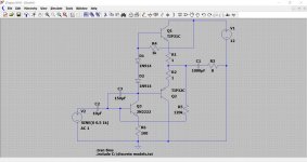
Going back to the circuit in post #1...
I tried simulating this (although I can't make out a lot of the values you used) and while it is 'poor' it should also work given a little tweaking.
In simulation it seemed to be much better (magnitudes better) with a couple of easy tweaks.
Firstly add a low value resistor such as 100 ohm in series with the emitter of the input transistor.
Secondly, don't connect the upper biasing resistor to the speaker but instead connect it to the supply.
You can then return the speaker to ground.
The two low value emitter resistors are important. I used 1 ohm here. Also adjust the value of (my) R5 to get around 5 to 7 volts at the junction of the 1 ohm resistors.
Attachments
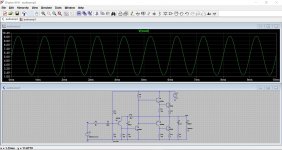
Funny, I played in simulation last night and came up with changes almost exactly as Mooly did, except I bootstrapped the collector resistor.
He he
 Its good when that happens
 C4 IS the bootstrap!
The output signal voltage is AC coupled to the base resistors "bootstrapping" them always to be above Vout.
This may not be intuitively obvious, but note that it is not possible to change the voltage ACROSS a capacitor without large charging currents being required. So Vout also appears at R3/R5 junction PLUS the DC bias there.
....don't connect the upper biasing resistor to the speaker but instead connect it to the supply....
Taken literally: this cripples the pull-up. You show 2V peak, but with a 12V supply we would hope for near 6V peak. The simple pull-up and one stage of current gain won't do well this way.
The cheap fix is, as said, a bootstrap. If the speaker is in the box, wires not exposed to user, speaker return to B+ is a time-honored hack. Added cap for bootstrap if speaker terminals are exposed.
Alternatively, turn the whole stage upside down and you can bootstrap from a groundy speaker. But now the input terminal references the noisy power rail. Adding another transistor can fix this... now it begins to be a "good" amplifier.
In any case, the resistor loaded class A driver is low efficiency and the class B output is high efficiency. With a single stage of current gain, the driver power can be very significant. We almost-always use two stages (Darlington) of output current gain. Also this significantly improves the bootstrap action.
Taken literally: this cripples the pull-up......
I know
The aim was just to keep it as simple as possible so that it made music. Nothing beats hearing audio from the first amp you cobble together. Every added component is another possibility for an error or problem.
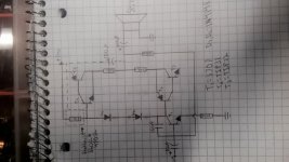
So I have finally replicated the simulations. I installed a 50K pot in place of the 150K feedback resistor, and when the voltage on the emitter-resistor junction is exactly 6.9V I would say it sounds great. This voltage fluctuates possibly in the positive direction so i'm thinking this might be caused by thermal instability?
Also, the 3707 heats up into motorboating after about 5 minutes so i'm assuming I should use a beefier transistor? alternatively, would more output devices take the load off of the 3707? I have found one configuration and drawn it in as T3 and T5, but alot of amplifier designs use 2 NPN transistors for the output devices like the example included. what is the best way of going about the addition of output stages?
Also, the 3707 heats up into motorboating after about 5 minutes so i'm assuming I should use a beefier transistor? alternatively, would more output devices take the load off of the 3707? I have found one configuration and drawn it in as T3 and T5, but alot of amplifier designs use 2 NPN transistors for the output devices like the example included. what is the best way of going about the addition of output stages?
Attachments
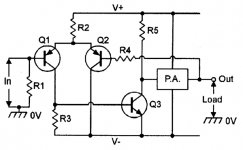
After some more studying of the BIPOLAR TRANSISTOR COOKBOOK I found the "voltage comparator type thing" I was referencing. So it seems if I wanted to implement this I should use a +/- 12V supply? although I read:
"The circuit can be used with a single ended power supply by grounding one supply line and using AC coupling of the input and output signals."
I was already planning on an input cap so this just means use ground instead of -V?
I'm sure R1 should be 1M, but how do I choose values for R2,R3,R4,R5?
I'm thinking a 3907 for the LTP and another 3707 for Q3, although I might just use a 3907 for Q3 + the first driver transistor.
Attachments
Last edited:
The thermal instability can be tamed by biasing T1’s base with a voltage rather than a current. Use a lower value feedback resistor, and tie another resistor from the base to ground. This forms a voltage divider. Pick the values such that 6-ish volts st the output node gives you vbe plus the right amount of drop across the 100 ohm emitter resistor. You want the current thru the bias resistors to be larger than the base current of T1, so that when beta and vbe drift over temp it doesn’t upset the bias point.
And if you do use CFP (or darlington, or quasi-comp) output stage, you can use small signal transistors to drive the outputs. A TIP driving a TIP may have high frequency oscillation problems which can cause weird symptoms if you don’t know what to look for.
And if you do use CFP (or darlington, or quasi-comp) output stage, you can use small signal transistors to drive the outputs. A TIP driving a TIP may have high frequency oscillation problems which can cause weird symptoms if you don’t know what to look for.
Great to hear you have it working 
My advice would be to build on what you have learnt and to stick with single rail designs for now. Although LTP configuration is the most widely used, it is far less forgiving of layout problems when breadboarding circuits. It is also used when dual rails (a plus and minus supply) is used because it allows for tight control of the DC conditions within the amp and allows a speaker to be coupled without using a cap (which for a beginner is risky because any problems can destroy the speaker as it is easy to accidentally allow full supply voltage across the speaker).
So I would advise to stick to AC coupled single rail for now.
The output stage using two NPN power transistors (as in your post above) is called a 'Quasi Complementary' type and it uses the PNP driver for the lower power transistor to try and emulate a PNP power transistor and driver. It originated in the early days of transistor amps when PNP output transistor were expensive and fragile and often poor performing. It is a great configuration and is still used widely today.
The emitter resistors marked 47 ohm 2 watt should actually be 0.47 ohm, not 47. Maybe the dot hasn't come out well
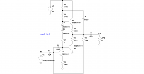
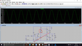
Here is a very simple design that adds a 'proper' output stage. This design runs with no quiescent current in the output stage... and it would be instructive for you to make something like this and listen to it. It is single rail and runs on your 12 volt supply.
The transistors are not critical and the output transistors can be the TIP31 types you show in post #1. Notice both are NPN's, so this is a Quasi Complementary design. Also notice the 10 ohm and 0.1uF across the output. As long as these parts are in the right ballpark they are not very critical.
This design can then be modified to overcome its 'no bias' condition and even go as far as changing it to use the complementary NPN/PNP type output stage. It could also be modified to incorporate an LTP type input stage.
Attachments
It is correct for now The diodes are a method of creating a fixed bias voltage between the base of the transistors, and that voltage is needed to turn the transistors on slightly so that they pass a little current under no signal conditions.
If we turn the volume down a little (reduce the input signal) the effect of this zero bias becomes apparent as the well known 'crossover distortion'. Can you tell by listening though?
Adding diodes to bias the output stage is only one method and although it is simple, it is also a little inexact. Two diodes isn't quite enough to get the stage to conduct properly, while three diodes generates to much bias voltage. The result is that the output transistors conduct heavily and get hot.
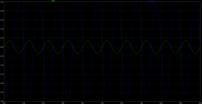
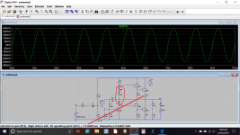
This shows the distortion of zero bias and then the problem of not quite enough bias (two diodes) and to much bias (three diodes).
The 1 ohm resistors are a big safety factor here. Don't try three diodes unless you are using 1 ohm emitter resistors.
The diodes are a method of creating a fixed bias voltage between the base of the transistors, and that voltage is needed to turn the transistors on slightly so that they pass a little current under no signal conditions.If we turn the volume down a little (reduce the input signal) the effect of this zero bias becomes apparent as the well known 'crossover distortion'. Can you tell by listening though?
Adding diodes to bias the output stage is only one method and although it is simple, it is also a little inexact. Two diodes isn't quite enough to get the stage to conduct properly, while three diodes generates to much bias voltage. The result is that the output transistors conduct heavily and get hot.
This shows the distortion of zero bias and then the problem of not quite enough bias (two diodes) and to much bias (three diodes).
The 1 ohm resistors are a big safety factor here. Don't try three diodes unless you are using 1 ohm emitter resistors.
Attachments
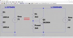
Instead of diodes we use this, a vbe multiplier. It consists of a transistor and a fixed and preset resistor.
By altering the preset we can set any voltage we like, and not only that, by having the transistor in thermal contact with the heatsink we can achieve a good measure of stabilisation against temperature changes.
In other words, as the output transistors get hot and would begin to conduct ever harder as temperature rises (a thermal runaway effect), this method will counter that. The increased temperature causes the voltage across the transistor to fall and that in turn automatically turns the output stage current down.
(Ignore the grounds on the simulation, they are just reference points for the sim to work)
So your two (or three or four diodes) are replaced by one of these and the preset is adusted to give an appropriate current in the emitter resistors (the 1 ohms). Around 20 milliamps would be fine for a little test circuit like this.
Attachments
I noticed in your design, Mooly, there are no diodes between Q3 and Q4 base....
It is "safe". It will work.
I have used a lot of gear which ran no-bias.
It avoids the very real problem in experimental work: not having any limit on bias and smoking your transistors instantly.
One of my old diagnostic techniques was to short-out whatever bias scheme the amp had, so I could find any other problems.
- Status
- This old topic is closed. If you want to reopen this topic, contact a moderator using the "Report Post" button.
- Home
- Amplifiers
- Solid State
- Transistor amplifier design