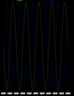
The attached plot shows the emitter current of Q2 and voltage at the node between Q2 E and Q4 C. What is going on with the wiggle at the bottom of the current plot? I see the same thing at Q4 E but 180 degrees out of phase obviously and everything looks fine in the load resistor.
Thanks,
Marty
Thanks,
Marty
Attachments
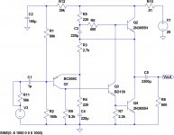
That connection between the emitter of q2 and collector of q4, and the junction of C3 and R3 is weird. If you look at the JohnE Basic50, and the Apex AX6 Retro Amp 50W Single Supply - Page 22 - diyAudio
they run the feedback back from that point to the emitter of the input transistor Q1. The AX6 schematic is on page 1 of that thread or somewhere close. AX6 also runs feedback from the output of the final capacitor to the emitter of Q1 through a resistor & a DC blocking cap.
This schematic is primitive anyway, with no emitter resistors to prevent the output transistors from thermally running away. Two drivers works better also, in a day when driver transistors cost $1 instead of $10 like in 1974.
Thanks for all of the replies. It works the same way with a couple of 3055 models I have both of them below. The swing at the output is 7.82 volts peak. Taking C3 to ground fixes the current waveform but the distortion at the output goes up considerably. Reducing C3 to 4.7uf fixes the simulation. I have no idea why it works though. I should mention that normal loads in the 4 to 15 ohm range I don't see any of this.
.model 2N3055 NPN(Bf=73 Br=2.66 Rb=.81 Rc=.0856 Re=.000856 CJC=1000P PC=.75 MC=.33 Tr=.5703U Is=2.37E-8 CJE=415P PE=.75 ME=.5 TF=99.52N NE=1.26 IK=1 Vceo=60 Icrating=10 mfg=STMicro)
.MODEL 2N3055H NPN(IS=2.37426e-14 BF=129.119 NF=0.85 VAF=31.1252 IKF=0.990922 ISE=2.47498e-10 NE=1.89002 BR=1.01252 NR=0.924456 VAR=254.624 IKR=2.70227 ISC=2.47498e-10 NC=2.90624 RB=3.66609 IRB=0.1 RBM=0.1 RE=0.000352673 RC=0.0764459 XTB=1.34801 XTI=1.07207 EG=1.206 CJE=9.03089e-08 VJE=0.513954 MJE=0.59999 TF=1e-08 XTF=1.36696 VTF=1.02605 ITF=0.987296 CJC=5e-10 VJC=0.400243 MJC=0.410238 XCJC=0.803124 FC=0.661216 TR=1e-07 VCEO=60 ICRATING=15 MFG=Motorola)
I think that's normal. Question is why the 600?
The top transistor is a CCS so it is always better if you can choose the lower transistor to be the one with higher HFE. Try the 2N3055H at the bottom. The BF=129 (versus 73 of the 2N3055) shows that it is of higher gain.
The top transistor is a CCS so it is always better if you can choose the lower transistor to be the one with higher HFE. Try the 2N3055H at the bottom. The BF=129 (versus 73 of the 2N3055) shows that it is of higher gain.
Last edited:
I think that's normal. Question is why the 600?...
The six hundred is for a pair of headphones. I like the way they sound hooked up directly to a real power amp so I figured I would give the JLH a try. I'm just playing around with the sim to get an idea of what might go wrong and and where to look to fix it if it does. My experience level is low especially with solid state but I have never seen anything like the current distortion showing up here.
I see. But for best result, there is another JLH circuit intended for driving headphone ") Or you can probably use a parallel power resistor to take the load impedance suitable for the amp. Small external module complete with protection... BTW, if you happen to have different hfe of the output stage transistors, put the high gain one at the bottom and it might solve your problem.
Or you can probably use a parallel power resistor to take the load impedance suitable for the amp. Small external module complete with protection... BTW, if you happen to have different hfe of the output stage transistors, put the high gain one at the bottom and it might solve your problem.
Or you can probably use a parallel power resistor to take the load impedance suitable for the amp. Small external module complete with protection... BTW, if you happen to have different hfe of the output stage transistors, put the high gain one at the bottom and it might solve your problem.
Last edited:
There was a broadly similar circuit to the JLH1969 for headphone use published in Hi-Fi News & Record Review in January 1979 issue.
You can find some later Class A headphone designs by Linsley-Hood at A Paul Kemble web page - John Linsley Hood preamp designs. I supplied some of these to Paul Kemble but the board layouts are not shown. I have the layouts for those other than that for the Chiara kit version.
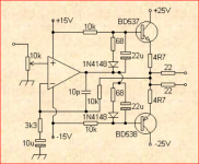
I still have the rather complex pre-amplifier published in Wireless World in 1982 which includes one of these headphone amplifier examples - this based around an IC op.amp and a couple of medium power transistors.
This could be built easily enough on project board on headphones the sound was something of an unforgettable surprise in view of the prevailing dislike of IC op.amps back then.
The quoted distortion is <0.01% on all loads down to 8 Ohms up to 3 volts rms output. The supplies for the IC are +/-15 V while the discrete output stage draws 40-50 m.a. from +/- 25 V. The transient response is also smooth both with resistive and reactive loads.
I did make up some boards for the discrete component version published in ETI in June 1984 but I did not bother replacing this IC one to which I had become quite addicted.
You can find some later Class A headphone designs by Linsley-Hood at A Paul Kemble web page - John Linsley Hood preamp designs. I supplied some of these to Paul Kemble but the board layouts are not shown. I have the layouts for those other than that for the Chiara kit version.
I still have the rather complex pre-amplifier published in Wireless World in 1982 which includes one of these headphone amplifier examples - this based around an IC op.amp and a couple of medium power transistors.
This could be built easily enough on project board on headphones the sound was something of an unforgettable surprise in view of the prevailing dislike of IC op.amps back then.
The quoted distortion is <0.01% on all loads down to 8 Ohms up to 3 volts rms output. The supplies for the IC are +/-15 V while the discrete output stage draws 40-50 m.a. from +/- 25 V. The transient response is also smooth both with resistive and reactive loads.
I did make up some boards for the discrete component version published in ETI in June 1984 but I did not bother replacing this IC one to which I had become quite addicted.
Using a higher hfe part at Q4 fixes the current distortion at Q2 but Q4 still shows the distortion. Reducing the size of C3 seems to work well no matter if the outputs are equal or using the higher gain part at Q4. If C3 is too low the harmonic distortion at the output goes way up. (second is raised by 20dB or so at 1uF)
I have still have no idea why it does the weird frequency doubling thing unless I change C3 and maybe it is one of those things that won’t happen IRL.
Thanks for all of the suggestions for tested HPA designs, I know this is kinda the path less traveled as far as these things go but it seems to work and I had many of the parts so not too much of an investment for me to build it and I can always repurpose it later if I can’t get it working at the breadboard stage.
Thanks again,
Marty
If you want to use the amp both for speaker and hp, you can add dummy load just like traditional amplifier, to keep the load impedance around 8 ohm. But if you want to use it only for hp then you can modify the amp.
C3 is to make sure there is constant voltage across base resistor. This in turn create constant base current. This base current, with hfe, turns top transistor into constant current source to make distortion lower. But you cant just reduce the cap without affecting bass roll off. There is a minimum (RC) value.
To solve your current issue, i think you can reduce the overall gain, which you don't need much if only for hp. Or, may be you can move the bootstrap point closer to the rail. Your base resistors are 220 and 400, you can change this probably into something like 100 and 520. The total resistance determine the base current.
Hi Michael, can you tell us the particular Wireless World issue you refer to? We have an excellent archive at THE HISTORY OF RADIO documented in thousands of PDF books and magazines but sifting through the issues isn't cheap or easy.I still have the rather complex pre-amplifier published in Wireless World in 1982 which includes one of these headphone amplifier examples - this based around an IC op.amp and a couple of medium power transistors.....
Hi Michael, can you tell us the particular Wireless World issue you refer to? We have an excellent archive at THE HISTORY OF RADIO documented in thousands of PDF books and magazines but sifting through the issues isn't cheap or easy.
The circuit diagram is on page 63 of the November 1982 issue. The layout of the pcb is on page 80 of the February 1983 issue.
Many thanks for the directions. For quite some years, I've also enjoyed the major improvement of a low impedance drive for headphones. I'm looking forward to testing a lash-up of this one as I don't think I've ever tried anything quite as simple and potentially quite small. If it still works well enough, this always make things more attractive
On the negative peak, Q4 is turning Q2 back on because the 600 Ohm load does not draw all the Q4 current. You can adjust R7 so that Q4 comes on when Q2 Vb is at half V1, but this does not work when you have a reactive load or not exactly the predicted load value. A successful class AB output is designed so that the crossover can happen at any voltage. This is 2019 so I suggest you buy some xx2955 PNP power transistors and make this dog of a circuit into one that works well.
BTW, I have a circuit that uses only NPN transistors that simulates well, but it is only useful for chip amps where pnp transistors are a problem. Given the availability of good cheap PNPs, it's pointless.
BTW, I have a circuit that uses only NPN transistors that simulates well, but it is only useful for chip amps where pnp transistors are a problem. Given the availability of good cheap PNPs, it's pointless.
I have attached the circuit using a dual IC and a couple of medium power transistors that I mentioned earlier. It should work in Class A under most conditions - lower impedance headphones generally require a lower voltage swing which will allow the latter mode of operation.
Higher impedance headphones may require a power amplifier to drive them. So if there is a problem with that replace the 600 Ohm head phones with a low impedance set.
It seems from the discussion of a simulation the point of building the hardware has not yet arrived and I thought there might be some interest in a simple low cost way to resolve the issue - offsetting the cost of replacing the headphones.
Attachments
Err.rrh! JLH 1969 isn't Class AB but full Class AA successful class AB output is designed so that the crossover can happen at any voltage. This is 2019 so I suggest you buy some xx2955 PNP power transistors and make this dog of a circuit into one that works well.
I don't think you understand why it is still so popular.
Its THD profile, 0.1% almost pure 2nd, near clipping and reducing rapidly with level is one of the few 'inaccurate' amps that may actually be preferred .. even by true golden pinnae who recognise that it isn't fully 'accurate' in DBLTs.
It's quite difficult to replicate this THD profile .. especially with speaker loads. You should check this out in SPICE world and see if you can make a Class AB amp with your extra xx2955 to 'sound' as good.
If you want accurate, build an O2 amp.
Some of JLH's later headphone amps .. like the one mjona just posted ... may be 'Class A' but are quite horrible for a number of reasons and aren't accurate either.
Last edited:
Some of JLH's later headphone amps .. like the one mjona just posted ... may be 'Class A' but are quite horrible for a number of reasons and aren't accurate either.
Without stating these reasons I see your comments as a slur - you are not saying you have you actually built any of these circuits or listened to them.
I gave the specifications for the circuit in question in post 9 you have given no technical argument to counter Linsley-Hood's results.
What are you on about?
- Status
- This old topic is closed. If you want to reopen this topic, contact a moderator using the "Report Post" button.
- Home
- Amplifiers
- Solid State
- What am I seeing here?