Apex, I was wondering, is there a specific reason or benefit why the input and output connections of your HX11 amp are located in close proximity to another ?
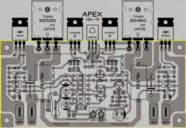
This PCB is not my design, it is designed by diyaudio member "willy"
I don’t understand the motivation behind a minimalist class G amp. By it’s very nature an amp of this type is going to be a relatively complex beast, with multitapped (or multiple) transformers, multiple rectifiers and smoothing networks etc. Plus there’s the additional speed and OLG needed to ensure distortion products are well suppressed as the amp switches to the higher supplies. So IME an amp of this type with 13 transistors and a single sided PCB is only going to result in frustration and mediocre performance.
I don’t understand the motivation behind a minimalist class G amp. By it’s very nature an amp of this type is going to be a relatively complex beast, with multitapped (or multiple) transformers, multiple rectifiers and smoothing networks etc. Plus there’s the additional speed and OLG needed to ensure distortion products are well suppressed as the amp switches to the higher supplies. So IME an amp of this type with 13 transistors and a single sided PCB is only going to result in frustration and mediocre performance.
It would be a good sub amp.

With a high quality SMPS for both low/high rails and a better design , I intend to go "audiophile" !!
8 transistors - that is my OPS and 12 for the IPS. (20)
Yes , I agree ... 14db 20Khz extra gain margin is needed for just the AB inner pair. One needs to negate the 2 switch - on points of the class G. I eliminated that , too.
My outer pairs always conduct 20ma minimum.
Crest uses a D-pac dual soft switching schottkey with- out any calculated
snubber network. And they switch , as well. This gives them .1% (full power 1k thd).
20 devices is not "complicated". Without class H switching , better snubbed
low rail diodes , and the "bad a$$" CFA stage .... 30ppm at full power.
My simulated Triple EF3 gives 20'ish PPM @ 20K.
I simulated that NAD , really good. But it switched ... I could not track 200Khz class H. But , it is the best OEM class H I reverse engineered yet.
I would welcome any criticism of this design. I have actually built and
used most of it , except for the CFP trackers (Crest).
PS - output/driver devices will be faster Sanken's. Maybe even MT-200's !
I looked at Self's class G kit (intensely) , in my opinion it IS that sort of "minimalist" design as you speak of now. None of the class H extra distortion
mechanism's are addressed. Layout and basic circuit is better , but not acceptable to me.
OS
Attachments
Last edited:
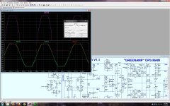
Havent really looked at the input bit, but the output stage looks very well thought out. have you got any waveforms showing the voltage on the output stage collectors? It’d be interesting to see how the 22p and 150p networks dictate rise/fall times of the supplies.
C111/112 allows me the "shape" rise/ fall with the bypass of diode Ct/driver Ccb.
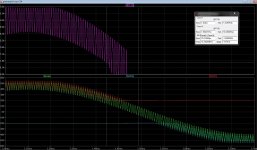
In the plot (below 2) is the R116 current (pink-no switching) , red and blue are the class H trackings.
I would most likely have to "tune" C111/112 and R121 to the specific devices I
end up using. Most models (even slow mje15032/33) work perfectly.
C111 even mitigates most of the reverse leakage "glitch' of D103 ,and R121 even
mitigates the much larger switching of the low rail diodes.
Using Infineon soft switching schottkey models for D103 and D106 - no "glitch' at all.
D106 will be a Infinion dual parallel 6A D-pak schottkey - like Crest uses.
Q111 refines impedance and voltage to give a superior reference. Reduces
D103 glitch , as well.
The result is worst case "difficult tracking' becomes quite easy (below 1) clipped 1k
with 200khz carrier .
The CFA's 200V/uS slewrate is also "easy" to negotiate. My goal was to
match or exceed my standard Sanken based EF3. The EF3 could slew to
almost 400V/uS with 60mhz Sankens ... could not match that .
But most is overkill. Also, Relatively simple for this level of performance.
Lots of pretty LED's ... too. Clips like a Valve ,as well.
Edit - full power 20Khz @ 42ppm. The EF3 was 20K@ 20PPM. The class G adds 20ppm , early effect +
imp. changes on the floating rails. But I was comparing this to a 10 device EF3 simulation.
OS
Attachments
Last edited:
Just picking up my thread from last year:
I'm still not sure what design to build, as each one is lacking reliable SOR protection.
Another question, regarding the PSU: As said before, I've got two identical transformers with 26-0-26 Vac secondaries. Is it preferable to wire the secondaries in series to get 52-26-0-26-52 Vac and rectify the lower and the higher rails with two bridges, or should I better rectify each transformer and connect both 35-0-35 Vdc voltages in series? In both cases the result will be 70-35-0-35-70 Vdc rails.
Best regards!
Rectify each individually, then connect the resulting supplies in series. The idea behind this is that you more fully engage the transformer windings, all the time. When drawing off the + (or -) 35, you’re operating off a 2-diode center tapped rectifier using both halves of the transformer. This gets you 70% of the trafo rating, as opposed to only 50% if you operate off only half of a given transformer with the upper half unused, which is what happens with just an inner bridge and an outer bridge. You get full VA capability off the upper rails of course, but you spend a lot of time on the lower ones.
Well, that sounds . This will basically give a daisy chain of four filter 'lytics. Would you recommend to add chain of two for the outer rails?
Back to Aniket's design at the 1st page. I recogniz a current limiting device that senses the voltage drop over R29. Ist this sufficient to protect all power devices in any overload situation? If I'd add a real SOAR protection, where is the best place for it? Across the Vbe multiplier or across R42?
Best regards!
. This will basically give a daisy chain of four filter 'lytics. Would you recommend to add chain of two for the outer rails?Back to Aniket's design at the 1st page. I recogniz a current limiting device that senses the voltage drop over R29. Ist this sufficient to protect all power devices in any overload situation? If I'd add a real SOAR protection, where is the best place for it? Across the Vbe multiplier or across R42?
Best regards!
Attachments
Last edited:
Current sensing is usually just done across the emitter resistor because it allows you to directly shunt the drive signal to the output when the limit is reached. It is also more complicated to sense both output current and Vce if you’re doing it across the vbe multiplier or thru a current transformer directly in series with the speaker. Anything can be done if you’re willing to resort to programming a PIC (and rely on a running computer program to protect your amp). But in terms of an analog circuit simpler is better and less stages and steering devices the more stable it is.
As much as people hate them, regular ordinary VI limiters tend to work quite nicely for class G (H) amps. Especially when using multiple breakpoints using the rail voltage taps, taking advantage of the fact that full voltage and full current can never appear simultaneously with this type of amp, even driving a pure zero power factor load.
As much as people hate them, regular ordinary VI limiters tend to work quite nicely for class G (H) amps. Especially when using multiple breakpoints using the rail voltage taps, taking advantage of the fact that full voltage and full current can never appear simultaneously with this type of amp, even driving a pure zero power factor load.
Where is miller capacitor.what is its work?330pf miller capacitance ... wow.
UG point must be 100k !!
Surely this design could be better at 68p or something reasonable.
OS
And what is UG point and why and how it must100k ?
Please explin me .i want to learn electronics really please help me.thanks
Miller capacitor is the capacitance between the base and collector (or source and drain) of a transistor. It's generally the capacitance that dictates the speed at which the transistor can operate.
A robust method of compensating an amplifier (reducing it's gain at high frequency to ensure it doesn't have gain at the point where the phase response is 180˚) involves placing an additional capacitor across collector-emitter of the VAS (or voltage amplifier stage) transistors. In fairly conventional amplifiers the VAS transistors have their emitters tied to the power supply rails via resistors that set the stage current, and the bases are driven from the preceding stage loads. Their collectors are connected together, with a resistor or Vbe multiplier between them. The collectors also go to the output stage, which is often an emitter or source follower to provide current gain but no voltage gain to drive the load.
Usually the output stage is very slow, as the transistors used there are physically large and have a lot of capacitance. If the preceding stage is too fast, the amplifier can get to a point where it's error correction gets out of phase with the drivers, and then rather than correcting any errors the amplifier instead amplifies them, and the whole lot oscillates.
UG point refers to Unity Gain point. This is the frequency at which an amplifier with its feedback network left disconnected (in an AC sense) drops to a gain of 1 due to the capacitances (generally miller capacitance) in the amplifier itself. Beyond this point we do not care (much) what the output phase does, as the gain is less than 1 so we cannot have an oscillator. Of course it can still ring, but that is less troublesome.
If you look at ostripper's plot in post #31, you'll see the open-loop gain of the amplifier is 80dB at DC. While not great, the 63ish dB excess gain (open-loop gain - desired closed loop gain) allows the amplifier to correct errors in it's output to the 0.001-0.01% level. However by the time we get to 20KHz, the amplifier runs out of excess gain. Errors will not be corrected, and the amplifier will distort very audibly.
The overall distortion performance is dictated by how well the amplifier individual stages can be linearised, so they don't distort in the first place, and how much excess gain it has to correct the inevitable errors.
These amplifiers aren't great to learn the basics of compensation, as they have extra complexity due to the rail switchers. A typical 3-stage (input diffamp, VAS, follower output) amplifier is generally the best to look at to get the fundamentals.
Last edited:
Where is miller capacitor.what is its work?
And what is UG point and why and how it must100k ?
Please explin me .i want to learn electronics really please help me.thanks
Miller effect - Wikipedia
That explains it all. Even subsearch within the wiki.
Adding capacitance limits amp bandwidth further. My new subamp uses 390pF !! , but just has to amplify 20 - 150hz. (200k+ unity gain BW).
Most of the common Toshiba (2sc/2sa) , BCxxx devices we builders use
will top out at 800khz to 1Mhz ... with a 47-68pF capacitor.
1Mhz ... we can't hear that !! But , that allows a lot of gain at 10-20Khz.
Why use the cap ??
To limit the bandwidth to the point (well) before the amps phase reaches 180 degrees ... you would then have positive feedback - an oscillator !
Older amps (with slower transistors) needed smaller caps to do this. The old
transistors had much more internal capacitance.
OS
- Status
- This old topic is closed. If you want to reopen this topic, contact a moderator using the "Report Post" button.
- Home
- Amplifiers
- Solid State
- I'm in search of a class G or H amplifier design