IPS or OPS ?Hi os you must try parallel capacitor on r25 , 100nf..10uf
Wait till I re-lable the OPS ( R101 /C101 / Q101) , that is the finished "standard".
OS
On the Crest -So the class G solution comes form Crest CC1800 amplifier:
2 schottky's in parallel for low rail ? Is this advantageous ?
But .... no R/C to mitigate the switching ?
OS
IPS or OPS ?
Wait till I re-lable the OPS ( R101 /C101 / Q101) , that is the finished "standard".
OS
Ips (68k)
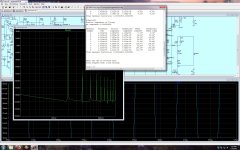
I have simulated successfully , but more THD and "glitches" beyond 10k.
 strange, I almost do not see hf harmonics... this is the first time in gnfb amp I can see hf harmonics are descending so quickly
On the Crest -
2 schottky's in parallel for low rail ? Is this advantageous ?
But .... no R/C to mitigate the switching ?
OS
The 6CWQ10FN is double diode in a single package. This is the reason of the paralelling.
I don't know the reason why the snubber is missing...
Sajti
That was before I fixed a reversed driver in the OPS. Now (below).
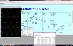
14ppm with class G - 20K , near full power /4R.
Look again below , there are some H7+ , 2nd is dominant.
Veysel - .1u to 10u parallel with R25 .... no effect - explain ?
So close , should I even add error correction or non-switching
to the OPS ??
OS
Attachments
6CWQ10FN - https://www.vishay.com/docs/93318/6cwq10fn.pdfThe 6CWQ10FN is double diode in a single package. This is the reason of the paralelling.
I don't know the reason why the snubber is missing...
Sajti
Better specs than most Schottky rectifiers , D-pac will be easy for
my first prototype PCB.
OS
But have they gone to the next level ?
- Very few schema's show snubbering / switching considerations.
- Even as they can "belt out" the efficient high power , they do it with
less than audiophile quality.
Edit - they try to compensate through careful selection of semi's , at best.
My plain class G (EF) and your simulation (CFP) , even as they do better than the
OEM ones I have made (simulated) .... still fall short.
I have (almost succeeded) in making the (class B) steps non-switching.
POS/NEG step semi's idle at 20-30ma. The class G steps switch
mid - waveform when the inner pair are already heavily conducting ,
much more evident then the inner pair at crossover. 4 extra bigger xover
like distortions for NFB to hopefully negate (which it can't) - fully.
Emotiva and other audiophile class G OEM's have secret IP class G - ooh!!
They even produce the step controllers as potted modules or leave
the steps blank in the official schematics - JERKS !
I am going to make my steps into beta enhanced voltage controlled current sources.
This will at least negate the extra 4 class G switch points.
I could go further and just make all 4 OP devices non-switching.
I think I have read enough to do both.
OS
Last edited:
Two things you can do with class G that help with the commutation noise. First, take a page from optimizing class B in general - which is to keep the drivers conducting well on either side of crossover. In normal class B, this means biasing the drivers relatively high. You’re probably going to do this anyway. Do the same with the rail switches - never let them turn off even when they don’t supply current to the load. Have a minimum load of 20, 50 mA or whatever it takes hanging off their emitters. Then they do not turn on abruptly when switching from the low rail to the high - it just starts increasing the current through the upper transistors, and the collector voltage of your outputs begins to rise. The other suggestion is to use schottky rectifiers, not regular ultra fast. Yeah, they are leaky and limited as to what kind of supply voltages you can use, but they do eliminate reverse recovery spikes. This will minimize the snubbering you need. Even a few mA of leakage is nothing if you “waste” 20mA or so biasing the slaves for faster turn on.
Do the same with the rail switches - never let them turn off even when they don’t supply current to the load. Have a minimum load of 20, 50 mA or whatever it takes hanging off their emitters.
I did some simulation about this solution, without any success. Maybe I was not careful enough, but there was no significant advantage to keep some bias current for the outer devices.
Sajti
I did some simulation about this solution, without any success. Maybe I was not careful enough, but there was no significant advantage to keep some bias current for the outer devices.
Sajti
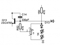
You think so ?? I succeeded . non- switching steps make this output stage "sing".
(Below) - positive step example.
- Steps always idle at 4-5ma , had to load the step rail (R50).
-(R32) establishes the bias , I might upgrade that to a simple CCS in case
of ripple in the higher 60v rail (or "settling" issues with the stepped rail).
-(R43/C18) filter was inspired by Hitachi.
-EF works better than CFP. More stable.
(D13) step voltage diode , if it is carefully snubbered (33pf/150R) can be
cleaned up further. Althrough , R32 as a CCS would mitigate the diode
switching , it is only nA level.
I swapped KT/Cordell/OEM drivers/outputs , all the same goodness.
2R , 100khz ,transients , clipping . No glitch , no problem.
I will try the CCS ,and a few more refinements.
Sajti - I have the exicon models , will design a Lateral version to match
this one.
OS
Attachments
Be careful with the thermal runaway of the outer device, wihth no emitter resistor, and resistive bias settings....
Sajti
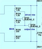
This OP stage uses the fancy harmon/kardon Vbe , with a second active device
(which could be adapted)for the outer device drivers.
I do agree ,aggressive high rail operation will require thermal FB.
I might add .22Re for the outer devices. The .1R was just to monitor current.
OS
No , this ...
OS
I recommended the diode triplet for the outer bias only...
Sajti
- Status
- This old topic is closed. If you want to reopen this topic, contact a moderator using the "Report Post" button.
- Home
- Amplifiers
- Solid State
- GreenAmp ++ modulated Class G output