I'm designing an audio amplifier and I have a few question. I'm hoping this type of post is okay, if not, please let me know I'll remove it ASAP.
Does my biasing of the output stage seem to be okay? I have about 3-3.2 V between the complimentary pair to eliminate crossover distortion, but I'm wondering how it could be improved.
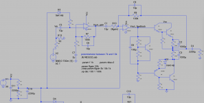
Sorry for the text being so small, the updated LTSpice on mac makes it super small. Also, in this schematic I have two of these things stacked on top of each other, and that's the wire you see hanging off towards the bottom left.
Thank you.
- I'm designing with a vcc of 30V.
- For my VAS stage I have two gain stages using a dual NE5532.
- For my current gain stage I'm using a complimentary symmetry pair with a npn darlington pair up top, and an pnp, npn CFP pair in the bottom.
- I have 2 ohm power resistors for emitter degeneration. The current running through these guys is about 200 mA, but power dissipation seems to still be about under a quarter watt.
- To eliminate crossover distortion, I have about 3-3.2 V in between the complimentary pair.
- For feedback, I'm filtering back frequencies below 24k. Is this an okay value, or should I be filtering back up to 100k for more correction?
Does my biasing of the output stage seem to be okay? I have about 3-3.2 V between the complimentary pair to eliminate crossover distortion, but I'm wondering how it could be improved.
Sorry for the text being so small, the updated LTSpice on mac makes it super small. Also, in this schematic I have two of these things stacked on top of each other, and that's the wire you see hanging off towards the bottom left.
Thank you.
Attachments
Last edited:
C2 & C3 where they are at 1000 uf seem extremely weird. Would short out AC output.
Real darlingtons are not respected in audio because there is not enough place for the base charge to go when crossing over zero. You have home built darlingtons, but the 1000 ohm resistor below the emitter of Q1 won't help bleed off base charge much.
3.2 v is too much crossover idle voltage. With 4 diode drops should be about 2.4 v. TO3 packages do okay with about 20 -30 ma of idle current, TO220 somewhat less. TO92 at 30 v would only be good for about 16 ma total current, your idle current would have to be a lot lower than that.
2n2222 outputs are going to be so feeble the op amps can do almost as well by themselves. While the metal case originals were 1 W parts the plastic copies available these days are 1/2 Watt. Upgrade at least to a $.30 TIP41C or something. What continent are you on? Particular transistor types available depend on the ordering habits of your suppliers.
Last edited:
It was explained to me that these kind of act like AC bypass? Kind of like, not affecting the DC bias.C2 & C3 where they are at 1000 uf seem extremely weird. Would short out AC output.
Are you recommending to design something instead like a class A or G amplifier instead? About the 1k ohm resistor, it was my understanding that it needs to be about 100x of the emitter degeneration resistors, so maybe I should change it to be about 200 ohms.Real darlingtons are not respected in audio because there is not enough place for the base charge to go when crossing over zero. You have home built darlingtons, but the 1000 ohm resistor below the emitter of Q1 won't help bleed off base charge much.
The reason I went up to 3.2 V is because I simulated it and it seemed to be completely eliminated around that voltage. Instead, do I just take the 4 diode drops and run with it? I was assuming you just up the voltage UNTIL crossover distortion is eliminated. I think the 3904's/6's are TO92, while the 2n2222's are TO-18,206AA's.3.2 v is too much crossover idle voltage. With 4 diode drops should be about 2.4 v. TO3 packages do okay with about 20 -30 ma of idle current, TO220 somewhat less. TO92 at 30 v would only be good for about 16 ma total current, your idle current would have to be a lot lower than that.
These are the 2n2222's that I'm using. Seems they are rated for 800mA max, I thought that would be enough but maybe I'm wrong. And I'm in the U.S.!2n2222 outputs are going to be so feeble the op amps can do almost as well by themselves. While the metal case originals were 1 W parts the plastic copies available these days are 1/2 Watt. Upgrade at least to a $.30 TIP41C or something. What continent are you on? Particular transistor types available depend on the ordering habits of your suppliers.
Thanks for your detailed response!
I hope this is not a school project. Your co-students should help you in the library or something. Glad to help a genuine new experimenter. This forum is mostly about class AB amps, although there are a few class A lurking about: For people IMHO who like to listen to their music at a lower volume than the traffic driving by. I like about 70-80 db. That takes about 1.5 W with 50 W peaks when the cannon goes off in 1812 Overture.
C2 & C2 short anything in audible range from one emitter to the other. So the highs of crossover distortion would squirt right out the speaker. Vertical edges of the transistor switching on or off have a lot of high frequencies. Look at some of the other threads, nobody bypasses the emitter resistor with a capacitor after the vacuum tube era. . TGM8, AX6, AX8 are about the simplest alt AB amps. .
Check your wattage rating of the 2n2222. The bond wires (Imax) can take a lot more than the die. Dies self heat, go into second breakdown, zot, you have a .5 ohm resistor. V*I=P and there is a limit to how many degrees per watt the package will slough off. TO92 are really ****y heat dissipaters. Heat sink flange transistors like TIP41C or MJE340, you can use heat sink compound, move the heat to the metal, the metal moves the heat out to the air. I use drilled & sawed window frame material on my budget sinks for VAS & predrivers. I use a lot of fans on heat shinks too, salvage from PCAT power supplies often. The ST-120 in my tag line tended to melt output transistors pretty frequently before I put in bigger heat sinks with fingers and blew fans on them. Had a 120 W rating for about 10 minutes if you didn't turn it on again for 12 hours.
Read wikipedia about high pass and low pass (electrical) filters. I'd say do the experiment and see what it sounds like on headphones. Horrible I imagine. Point to point on vector board or blank board, this is pretty simple.
Last edited:
I hope this is not a school project. Your co-students should help you in the library or something. Glad to help a genuine new experimenter. This forum is mostly about class AB amps, although there are a few class A lurking about: For people IMHO who like to listen to their music at a lower volume than the traffic driving by. I like about 70-80 db. That takes about 1.5 W with 50 W peaks when the cannon goes off in 1812 Overture.
C2 & C2 short anything in audible range from one emitter to the other. So the highs of crossover distortion would squirt right out the speaker. Vertical edges of the transistor switching on or off have a lot of high frequencies. Look at some of the other threads, nobody bypasses the emitter resistor with a capacitor after the vacuum tube era. . TGM8, AX6, AX8 are about the simplest alt AB amps. .
Check your wattage rating of the 2n2222. The bond wires (Imax) can take a lot more than the die. Dies self heat, go into second breakdown, zot, you have a .5 ohm resistor. V*I=P and there is a limit to how many degrees per watt the package will slough off. TO92 are really ****y heat dissipaters. Heat sink flange transistors like TIP41C or MJE340, you can use heat sink compound, move the heat to the metal, the metal moves the heat out to the air. I use drilled & sawed window frame material on my budget sinks for VAS & predrivers. I use a lot of fans on heat shinks too, salvage from PCAT power supplies often. The ST-120 in my tag line tended to melt output transistors pretty frequently before I put in bigger heat sinks with fingers and blew fans on them. Had a 120 W rating for about 10 minutes if you didn't turn it on again for 12 hours.
Read wikipedia about high pass and low pass (electrical) filters. I'd say do the experiment and see what it sounds like on headphones. Horrible I imagine. Point to point on vector board or blank board, this is pretty simple.
Got it. Yeah this isn't FOR school, but in an analog class we learned a tiny bit about audio amps and I wanted to try to build one myself. You could say I have zero background knowledge in AF Amp design other than some of the basics.
I have built something like this and it didn't sound terrible, but improvements definitely could be made, and that's why I'm here. What class would this circuit be? Class AB or B? What I've read is that the difference lies in the biasing, class B having exactly half conduction cycles, while AB has a little more biasing, and they crossover more. What direction do you recommend I take this in? You say that darlingtons are not respected in audio, are you suggesting that I buy a single discrete transistor to accomplish what I'm trying to do with the 3904/2222 pair?
Thanks for all your help.
By the time you have 200 mA of standing current in your emitter degeneration resistors, your 2N2222s are dissipating almost 3 W each - as mentioned, that's a tad too much for a TO-92 case. (They're pretty bad thermally, half a watt tops.) And since this still isn't a fully class A amplifier, that's not even maximum dissipation! You'd have to run a TRANsient simulation and plot VxI, I think you can have an average displayed after right-clicking or whatever that was.
Maximum output current would reach 1.5 A and change, so I'd shoot for at least a 3-4 A part like the ones mentioned and relegate 2N2222/2N2907 to driver duty (what your 2N3904/3906 are doing now). These are going to be either medium power in TO-126 (or surface mount DPAK or SOT-223), or higher power in TO-220, maybe TO-3P (I don't think there's too many in TO-264 until you hit 10 A or so). These are much better suited for heat transfer to a heatsink, though be warned that with the exception of all plastic case TO-126s, their metal tabs are generally at collector level and will require adequate insulation when strapping multiple ones to the same heatsink (traditionally provided by thin mica washers with the requisite silicone thermal compound, with silpads being a more convenient but also somewhat less well-performing alternative).
Yeah, the tiny default font size is a nuisance in LTspice XVII. For some reason, a bunch of things in "legacy" schematics will default to 0.625 size. You can often edit things manually but it's a PITA.
Bypassing emitter degeneration resistors is an interesting idea, though doing it throughout the entire audio band could result in slightly cumbersome capacitor values like 10000 µF (which, however, would also cope fine with ripple current levels required).
BTW, an ideal voltage source does not require filter capacitors.")
In any case, you should make up your mind on whether you want an A or AB output stage (which would depend on transformer, filter cap and heatsink stock at hand). For what a low wattage class A amp typically involves, see e.g. the classic JLH amplifier, a 10 W job. Emitter degeneration resistors are less critical in a class A, so 1 ohm would do fine there, in an AB you'd go with more like 0.47 ohms down to 0.22 (though the latter may be too low for good thermal stability if the drivers are off the main heatsink).
Maximum output current would reach 1.5 A and change, so I'd shoot for at least a 3-4 A part like the ones mentioned and relegate 2N2222/2N2907 to driver duty (what your 2N3904/3906 are doing now). These are going to be either medium power in TO-126 (or surface mount DPAK or SOT-223), or higher power in TO-220, maybe TO-3P (I don't think there's too many in TO-264 until you hit 10 A or so). These are much better suited for heat transfer to a heatsink, though be warned that with the exception of all plastic case TO-126s, their metal tabs are generally at collector level and will require adequate insulation when strapping multiple ones to the same heatsink (traditionally provided by thin mica washers with the requisite silicone thermal compound, with silpads being a more convenient but also somewhat less well-performing alternative).
Yeah, the tiny default font size is a nuisance in LTspice XVII. For some reason, a bunch of things in "legacy" schematics will default to 0.625 size. You can often edit things manually but it's a PITA.
Bypassing emitter degeneration resistors is an interesting idea, though doing it throughout the entire audio band could result in slightly cumbersome capacitor values like 10000 µF (which, however, would also cope fine with ripple current levels required).
BTW, an ideal voltage source does not require filter capacitors.
In any case, you should make up your mind on whether you want an A or AB output stage (which would depend on transformer, filter cap and heatsink stock at hand). For what a low wattage class A amp typically involves, see e.g. the classic JLH amplifier, a 10 W job. Emitter degeneration resistors are less critical in a class A, so 1 ohm would do fine there, in an AB you'd go with more like 0.47 ohms down to 0.22 (though the latter may be too low for good thermal stability if the drivers are off the main heatsink).
Last edited:
I suggest TIP41C/42C for output transistors, that have the power rating to exceed the current available out of the 5532. I use them for drivers, not fast enough to be ideal but very cheap & tough. You've violated the power rating of the 2n2222 output transistors. 16 ma * 30 v = 480 mw and 500 mw is the limit of purchasable 2n2222 with top dipped in a refrigerated water bath.
I suggest you delete C2 & C3. Enablers of cross-conduction, don't do anything for the sound.
Then build it. Be prepared to change the emitter resistor on Q1 to 100 from 1000, but do that version 2. You can tack a 150 across a 1000 after you listen to it as is. You can also tack C2 & C3 across your 2 ohm resistors after Version 1 is working. I think if you put a current probe in series with them, or a 0.1 ohm resistor or something, you might see significant current from one to the other. Cross conduction (which heats the transistors & doesn't help the sound).
Your VBE multiplier is fine (heat sensor transistor), you can reduce the resistance of the emitter pot as you go to see how it affects the voltage across the output emitter resistors. BTW people put a filter capacitor across the VBE multiplier, NOT the OT emitter resistors.
You can build this on wood or I use nema CE canvas-phenolic boards, tack wires on. Actual DIP boards are better for the op amp, it is hard to tack the wires on a socket direct without some spreading. Newark shut down mcmelectronics that had $2 dip prototyping boards, maybe they still have them on their website. Vero board is not cheap. Use a socket on the DIP, you can toast an op amp with a soldering iron easily. The sockets are tougher. particularly the $1 phosphor bronze ones from TE connectivity.
Don't forget 0.1 uf ceramic bypass caps on op amp rails. Within an inch of the op amp. Op amps need that. Buy a 22 or 33 pf caps for the feedback cap on the op amp, if you need more than 10 pf to stop oscillation you won't need to pay $8 freight to get it.
If you don't have a metal box to put it in, a 47 pf cap to short the inputs, and a zobel on output, expect to hear AM radio stations on your jewel. A zobel is a 11 turn inductor wound around a AA battery, parallel a 10 ohm several watt resistor. Keeps the AM radio from coming in from the speaker and going on the feedback line to the op amp.
Oh, use a $7 AM/FM radio as a sound source instead of a $200 cell phone. Accidents happen when prototyping. Blow up something cheap. Music out the earphone jack, and turn it down, radios can put 7 vac on a headphone.
Have fun.
Last edited:
What is D3 for??
As it happens, it does no harm with NE5532, but will flip-out with PNP-input opamps; FET may or may not go nuts.
What is C2 C3 doing? What is "Rdiss"? Oh, 2 Ohms? Driving 8 Ohms? Yes, no-C would lose 20% power, but with-Cs and push-pulling large output C2 C3 will charge-up and lose your hoped-for advantage.
R17 can only pull-down so far; long-story-short, output large-signal impedance is 2,700r/hFE(Q4 Q3) so a couple Ohms. There are better plans.
Major issue: the '5532 at that gain is flat to 3MHz. The big fat power transistors, probably somewhat less. Multiple high-cuts inside a NFB loop tends to be unstable.
As a "first" design, I have seen far-far worse. This one will "work", though perhaps riddled with MHz oscillations.
Hi sgrossklass, thanks for your reply. I'm thinking I will still design for class AB as it seems more interesting with figuring out the biasing, etc., then purely a class A. I'm hearing what you are saying about using the 2222/2907 as the driver duty, and that makes a lot of sense to me. The speakers I'm designing for are max rated at 10 W so I don't even know if that'll be necessary, I think I'll just use the TIP41C/42C's and ditch the darlington. I still need to make a new schematic and try my luck at designing, but I think I will keep the VAS stage. Thanks for your input.By the time you have 200 mA of standing current in your emitter degeneration resistors, your 2N2222s are dissipating almost 3 W each - as mentioned, that's a tad too much for a TO-92 case. (They're pretty bad thermally, half a watt tops.) And since this still isn't a fully class A amplifier, that's not even maximum dissipation! You'd have to run a TRANsient simulation and plot VxI, I think you can have an average displayed after right-clicking or whatever that was.
Maximum output current would reach 1.5 A and change, so I'd shoot for at least a 3-4 A part like the ones mentioned and relegate 2N2222/2N2907 to driver duty (what your 2N3904/3906 are doing now). These are going to be either medium power in TO-126 (or surface mount DPAK or SOT-223), or higher power in TO-220, maybe TO-3P (I don't think there's too many in TO-264 until you hit 10 A or so). These are much better suited for heat transfer to a heatsink, though be warned that with the exception of all plastic case TO-126s, their metal tabs are generally at collector level and will require adequate insulation when strapping multiple ones to the same heatsink (traditionally provided by thin mica washers with the requisite silicone thermal compound, with silpads being a more convenient but also somewhat less well-performing alternative).
Yeah, the tiny default font size is a nuisance in LTspice XVII. For some reason, a bunch of things in "legacy" schematics will default to 0.625 size. You can often edit things manually but it's a PITA.
Bypassing emitter degeneration resistors is an interesting idea, though doing it throughout the entire audio band could result in slightly cumbersome capacitor values like 10000 µF (which, however, would also cope fine with ripple current levels required).
BTW, an ideal voltage source does not require filter capacitors.
In any case, you should make up your mind on whether you want an A or AB output stage (which would depend on transformer, filter cap and heatsink stock at hand). For what a low wattage class A amp typically involves, see e.g. the classic JLH amplifier, a 10 W job. Emitter degeneration resistors are less critical in a class A, so 1 ohm would do fine there, in an AB you'd go with more like 0.47 ohms down to 0.22 (though the latter may be too low for good thermal stability if the drivers are off the main heatsink).
Hi indianajo, thanks for your continued engagement. I totally see now my flaw in energy budget, my 2222s will totally blow out. I like your advice about the op amp rails, I was not familiar with that, I will add some caps there. In terms of blowback protection, to not destroy my phones internals, can I throw in some sort of diode with some super high reverse bias voltage? Do you recommend keeping my VAS stage, other than the 22 pF or 33 pF caps, intact? I designed to filter back ~24k Hz, but am not sure if that's an optimal value or not. Thanks for your help.I suggest TIP41C/42C for output transistors, that have the power rating to exceed the current available out of the 5532. I use them for drivers, not fast enough to be ideal but very cheap & tough. You've violated the power rating of the 2n2222 output transistors. 16 ma * 30 v = 480 mw and 500 mw is the limit of purchasable 2n2222 with top dipped in a refrigerated water bath.
I suggest you delete C2 & C3. Enablers of cross-conduction, don't do anything for the sound.
Then build it. Be prepared to change the emitter resistor on Q1 to 100 from 1000, but do that version 2. You can tack a 150 across a 1000 after you listen to it as is. You can also tack C2 & C3 across your 2 ohm resistors after Version 1 is working. I think if you put a current probe in series with them, or a 0.1 ohm resistor or something, you might see significant current from one to the other. Cross conduction (which heats the transistors & doesn't help the sound).
Your VBE multiplier is fine (heat sensor transistor), you can reduce the resistance of the emitter pot as you go to see how it affects the voltage across the output emitter resistors. BTW people put a filter capacitor across the VBE multiplier, NOT the OT emitter resistors.
You can build this on wood or I use nema CE canvas-phenolic boards, tack wires on. Actual DIP boards are better for the op amp, it is hard to tack the wires on a socket direct without some spreading. Newark shut down mcmelectronics that had $2 dip prototyping boards, maybe they still have them on their website. Vero board is not cheap. Use a socket on the DIP, you can toast an op amp with a soldering iron easily. The sockets are tougher. particularly the $1 phosphor bronze ones from TE connectivity.
Don't forget 0.1 uf ceramic bypass caps on op amp rails. Within an inch of the op amp. Op amps need that. Buy a 22 or 33 pf caps for the feedback cap on the op amp, if you need more than 10 pf to stop oscillation you won't need to pay $8 freight to get it.
If you don't have a metal box to put it in, a 47 pf cap to short the inputs, and a zobel on output, expect to hear AM radio stations on your jewel. A zobel is a 11 turn inductor wound around a AA battery, parallel a 10 ohm several watt resistor. Keeps the AM radio from coming in from the speaker and going on the feedback line to the op amp.
Oh, use a $7 AM/FM radio as a sound source instead of a $200 cell phone. Accidents happen when prototyping. Blow up something cheap. Music out the earphone jack, and turn it down, radios can put 7 vac on a headphone.
Have fun.
Hi PRR, thanks for your input. You're going to laugh at me, but D3 is there as I was having the input signal from that node leak back into the Vcc/2 node. That's why I also have another fat cap across Vcc/2 to ground. My reasoning was, I have a small AC signal leaking into this line through the 10k, if I put a diode right forward biased, nothing will flow backwards through it. In the simulator it seemed to help, but I was not confident in its usefulness. I will take another look at the frequency response and try to cut down on oscillations. Thanks for your input.What is D3 for??
As it happens, it does no harm with NE5532, but will flip-out with PNP-input opamps; FET may or may not go nuts.
What is C2 C3 doing? What is "Rdiss"? Oh, 2 Ohms? Driving 8 Ohms? Yes, no-C would lose 20% power, but with-Cs and push-pulling large output C2 C3 will charge-up and lose your hoped-for advantage.
R17 can only pull-down so far; long-story-short, output large-signal impedance is 2,700r/hFE(Q4 Q3) so a couple Ohms. There are better plans.
Major issue: the '5532 at that gain is flat to 3MHz. The big fat power transistors, probably somewhat less. Multiple high-cuts inside a NFB loop tends to be unstable.
As a "first" design, I have seen far-far worse. This one will "work", though perhaps riddled with MHz oscillations.
Last edited:
My personal critique:
Don't try to share the voltage divider producing the midpoint. It'll only cause trouble. Remove R32, move R13 to the other side of C5, connect R32 to +V, connect R13 to GND. Make them both 47K.
Similarly add another voltage divider to the + input of the second opamp.
R17 should either be a constant current sink or a bootstrap arrangement. You can use the other side of C4 for this.
AS others have said, 2N2222 as outputs and 2N3904/2N3906 as drivers is a bad idea - but I suspect you used these because they were models available in LTSpice. Find out how to include SPICE models into LTSpice, it's not hard. BD139/140 as drivers and TIP3055 as outputs should work well for cheap experimenting.
So do you suggest still using a darlington pair? I've had conflicting advice here whether I should be using one or not. I'm designing for between 3-8 Watts, and I have the TIP41C/42C readily available to me.My personal critique:
Don't try to share the voltage divider producing the midpoint. It'll only cause trouble. Remove R32, move R13 to the other side of C5, connect R32 to +V, connect R13 to GND. Make them both 47K.
Similarly add another voltage divider to the + input of the second opamp.
R17 should either be a constant current sink or a bootstrap arrangement. You can use the other side of C4 for this.
AS others have said, 2N2222 as outputs and 2N3904/2N3906 as drivers is a bad idea - but I suspect you used these because they were models available in LTSpice. Find out how to include SPICE models into LTSpice, it's not hard. BD139/140 as drivers and TIP3055 as outputs should work well for cheap experimenting.
I having an issue seeing this R32 you're referring to?
R17 to the other side of C5, as in in between the cap and the load?
Thanks for your help.
Also, I do know how to import LTSpice models, etc. Not my first time using it.
Last edited:
Q1 & Q4 are drivers. I don't see getting rid of them, although upgrading to transistors with heat sink is traditional. MJE340 for Q1 & Mje350 for Q4 are popular. Since both outputs are npn you can use TIP41C for both. Another advantage of separate drivers over having them built into darlingtons is that heat in the output transistor does not flow immediately to the driver - causing it's gain to increase, causing "thermal runaway". Hint, do not put Q1 & Q4 on the heat sink with Q2 & Q3. Separate them.
One usually handles music on the power supplies by increasing capacitance. All electrolytic doesn't help because wound capacitors have inductance. Ceramic caps in parallel short out the higher frequencies that are held out of the electrolytic cap by inductance.
After your amp is working and not putting DC voltage or AC oscillation on the input jack, maybe it will be safe for your cell phone. Amateurs do not make 100% secure solder joints, and a popped loose wire can cause DC to reflect to either input or output. Your output cap helps protect your speaker - always a good idea IMHO for a first amp.
Oscillations do not occur as often in sims as they do in real life. Parallel wires have 8 pf/inch capacitance, as much as your anti-oscillation 10 pf cap. Good layouts have the inputs on one end of the board, outputs on the other end, and no long parallel runs. The feedback trace or wire requires particular intrusive management.
View sggrooklass and PRR as the design experts they are. I'm more an expert on low buck builds. If you put together a bill of materials, including your tools, I'll review it for you. You need a drill & some files for holes in an enclosure. Metal recipe files are great, obsolete but available at charity resale shops. PCAT power supply cases are good, come with a built in fan. Your heat sinks are too high to squeeze this in a Altoids box. You'll need a soldering iron and rosin core tin-lead solder. Plus safety glasses.
Best of luck.
Last edited:
Nothing wrong with using darlingtons.. though I would question why you want to use a quasi-complimentary output. I would probably go with the EF Type II arrangement (see Doug Self Distortion In Power Amplifiers - Home Warranty Appliances) but for this sort of thing it's not too critical.
Actually repairmen on PA equipment forum have made a lot of money replacing darlingtons in amps. The shop owner in Piraes GR has particularly commented on this.Nothing wrong with using darlingtons.. though I would question why you want to use a quasi-complimentary output. I would probably go with the EF Type II arrangement (see Doug Self Distortion In Power Amplifiers - Home Warranty Appliances) but for this sort of thing it's not too critical.
I'd say there's nothing wrong with quasi-comp. The distortion is down in the tenths of a percent IMHO which is not audible on actual speakers. Quasi comp also lends itself to speaker caps, which protect the speaker from amateur quality soldering skills at a cost of $2 and 1 square inch of board space. Speaker caps also protect from overheat errors of the output transistors which can happen with cheap heat sinks and no fan. Great for starting out in this hobby. Plus single supply requiring a speaker cap allows a 10 W amp like this to use a $10 doorbell tranformer (24 v) from the home supply, instead of a $30 dual winding toroid without a vertical mount flange which requires $8 freight from a specialty supply like antekinc.
Last edited:
Actually repairmen on PA equipment forum have made a lot of money replacing darlingtons in amps. The shop owner in Piraes GR has particularly commented on this.
I'd say there's nothing wrong with quasi-comp. The distortion is down in the tenths of a percent IMHO which is not audible on actual speakers. Quasi comp also lends itself to speaker caps, which protect the speaker from amateur quality soldering skills at a cost of $2 and 1 square inch of board space. Speaker caps also protect from overheat errors of the output transistors which can happen with cheap heat sinks and no fan. Great for starting out in this hobby. Plus single supply requiring a speaker cap allows a 10 W amp like this to use a $10 doorbell tranformer (24 v) from the home supply, instead of a $30 dual winding toroid without a vertical mount flange which requires $8 freight from a specialty supply like antekinc.
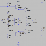
I'll definitely send you a BOM later when I get around to actually building this thing. I'm whipping up a new schematic with a bunch of improvements, and I'll post it here, maybe you can take a look at it. I'm still figuring out the op amp stuff, but here's the basic output stage. The 1ks send a ~ 13 mA current down that branch, turning on all the diodes, 2.8 V drop across there, and the drivers are biased to 700 mA Ic, which puts them into that okay region, I think?
Any suggestions?
Attachments
I don't see the feedback tap on this schematic. Feedback compensates for the non-linearities of transistors.
You need some sort of device to force the op amp to operate at the center of the power supply. Center tap of the transformer, (expensive, cheap doorbell transformers don't have one), op amp called a "DC servo", stack of zener diodes current limited by resistors, one voltage regulator IC (7815), something.
I'd go with higher output transistors emitter resistors than 0.22. That value is fine for people that are sure of their heat budget, but for first trials 0.47 ohms or 1 ohm is safer.
Dumping the base charge of the output transistor as it shuts off onto the emitter of the other driver transistor is non-traditional. Designers usually split the r3 and dump that to the power supply.
There are threads that show how to increase the output current of an op amp to make a low watt amp out of it. Let me see if I can find one. Edit, this is essentially the Peavey PV-4C only one pair of output transistors and lower rail voltage. Which see schematic. Didn't save them because 28 W is too low for my purposes. Usually one can get half or less the power supply out the speaker, so 15 v squared is 225, divided by 8 is 28 W.
One usually parallels one of the diode stack with a pot with wiper shorted to one end, so that one can turn down the idle bias current in the output transistors. Diode stack is usually mounted above the output transistor heat sink to collapse the spread voltage automatically due to negative heat coefficient of diode on voltage.
5532 can't drive 500 ohms, which is parallel combination of R5 & R6. Plus current coming from the driver bases. Cut those resistors to 2 k or more.
Last edited:
Okay, I hear you. I can post the rest of it later, I just haven't really designed the op-amp VAS stage exactly yet. For below 10 W, do you think I can get away with only 1 set of TIP41C/42C, or is the darlington still necessary? Ill change the emitter resistors, and if the darlington stays, I'll split R3 into two 100 ohms going to ground.I don't see the feedback tap on this schematic. Feedback compensates for the non-linearities of transistors.
You need some sort of device to force the op amp to operate at the center of the power supply. Center tap of the transformer, (expensive, cheap doorbell transformers don't have one), op amp called a "DC servo", stack of zener diodes current limited by resistors, one voltage regulator IC (7815), something.
I'd go with higher output transistors emitter resistors than 0.22. That value is fine for people that are sure of their heat budget, but for first trials 0.47 ohms or 1 ohm is safer.
Dumping the base charge of the output transistor as it shuts off onto the emitter of the other driver transistor is non-traditional. Designers usually split the r3 and dump that to the power supply.
There are threads that show how to increase the output current of an op amp to make a low watt amp out of it. Let me see if I can find one. Didn't save them because 28 W is too low for my purposes. Usually one can get half or less the power supply out the speaker, so 15 v squared is 225, divided by 8 is 28 W.
Getting the "ground" is the trick. Center tap transformer is at least $10 more than a 24v doorbell transformer, probably best bought from antekinc.com or someplace.
Base capacitance of a TIP41 is probably more than a 5532 can drive, although it is not on the datasheet. Getting the output transistors to shut off at zero crossover is an art, requiring a "hot" driver. If the turn off is slow because of limited driver current, the output slew rate is low and distortion happens on high frequencies. I'd say use 2n2222/2n2907 as your drivers at least. BD139/140 (2W), or MJE340/350 (10W) are popular drivers. See comment about PV-4C above, an amp with op amp, predriver, output transistors.
BTW I bought a blown up PV-4C for $20 +$28 freight on E-bay. comes with center tap transformer metal case, fan, great heat sinks, lots of transistors & diodes burned to sand. 65 v CT transformer, though. Watch the location, UPS charge was only $28 because distance was only 140 miles.
Last edited:
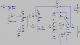
Drivers - first pairGetting the "ground" is the trick. Center tap transformer is at least $10 more than a 24v doorbell transformer, probably best bought from antekinc.com or someplace.
Base capacitance of a TIP41 is probably more than a 5532 can drive, although it is not on the datasheet. Getting the output transistors to shut off at zero crossover is an art, requiring a "hot" driver. If the turn off is slow because of limited driver current, the output slew rate is low and distortion happens on high frequencies. I'd say use 2n2222/2n2907 as your drivers at least. BD139/140 (2W), or MJE340/350 (10W) are popular drivers. See comment about PV-4C above, an amp with op amp, predriver, output transistors.
BTW I bought a blown up PV-4C for $20 +$28 freight on E-bay. comes with center tap transformer metal case, fan, great heat sinks, lots of transistors & diodes burned to sand. 65 v CT transformer, though. Watch the location, UPS charge was only $28 because distance was only 140 miles.
Output - Second pair
Correct?
If I tried to ween the base charge off in between the driver and outputs, with the 100 ohm to ground from each side, it started drawing an insane amount of current, I don't think I was doing it how you were suggesting.
Op amp gain - 22/7.6 * 22/7.6 = 2.89 * 2.89 ~ 8.35 voltage gain
From max signal from phone - 8.35 * 0.7 = 5.84 output voltage
Max power - after doing calculation it seems to be only around 2.1 watts, and thats not even average, I think i need to up the gain a little bit. Any blaring suggestions?
I really think I could improve how I get those opamps to Vcc/2, I think that's what you were describing earlier but I'm still a little unsure.
Also, change all the 47k's to 10k, i'm realizing now in this sim, Ic for the outputs is only 78 mA, that seems kind of low yeah?
EDIT: yeah this design doesn't work right now, it's working as an attenuator HAHA, but I'm still playing around with it.
Attachments
Last edited:
- Status
- This old topic is closed. If you want to reopen this topic, contact a moderator using the "Report Post" button.
- Home
- Amplifiers
- Solid State
- DIY Amp Design Critique