One thing is gain on U2 is Rf/Ri and I think your Ri is zero. R13 & R15 are some sort of ground reference but I think you need a Ri from + to C14. Say to make gain on U2 2 or less.
I also suggest you have a better ground reference than R13 & R15, either a center tap to a transformer, or a 15 v regulator from the 29 v rail (24 v *1.4)-1.2v . Then that could go in the middle of R3.
spice knows how much junction capacitance is in transistors, the peak current from a power transistor like TIP41 should be pretty high turning off. Why one uses smaller transistors with less BE capacitance for drivers.
Q3 Q4 Q1 Q2 are just current boosters, you'll get no voltage gain out of them. The op amp can swing voltage wise as much as 0.5*vcc - a couple of volts, that should be enough to drive a speaker. Current drive on Q3 & Q4 is mostly R5 & R6, the op amp just steers them from the middle.
Gain 8 on U1 is probably fine, 2 vac out of phone/radio, * 8 is 16 v swing, less about 1 for diode drops, 28 w like I calculated above.
That's it for today.
Because you have gain of infinity on U2, no wonder the output is banging between the rails from the feedback.
I'd say delete U2 as a signal component and use it as the center voltage ("ground") driver. Make it unity gain (no feedback resistor, output to minus pin) and connect plus to the 47 k voltage divided from +29v and - rail. Bleed in from a high resistor input the input.
Then run the feedback from speaker cap input to a mixing point at inverting pin of U1. Connect output of U1 to the bases of the drivers. That is how Peavey does it in the PV-4C. They bypass the feedback resistor with a 10 pf ceramic cap.
BTW 2n2222 2n2907 have low enough capacitance to be driven by a 5532, but they are noisy little switching transistors. mpsa05/55 are amplifier transistors. If you Private Message your US mail address, I'll send you free five pnp mpsa55 I paid $.024 for and five mps8099 I paid $.082 for. If you can't find a simulation model for mps8099 use mpsa06. Or mpsa06, mpsa56, models for both, those are higher voltage (80v) versions of the mpsa05/55 (60 v).
c3, c4, c5, c6 as power supply bypass caps should be 0.1 uf or at least 0.01 uf ceramic. And they don't connect pins 4,8 of op amp to the supplies, they parallel the supply inputs of the op amp.
Last edited:
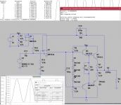
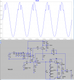
Okay, I think I'm finally getting somewhere. Take a look at this:
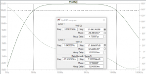
Max current drawn from voltage source: 960 mA
Feedback resistor: LP -3dB Point at 15.7k Hz with 56k and 200p
Inverting input resistor: HP -3dB Point at 2.84 Hz with 5.6k and 10 uF
Let me get up a mag response. I'm also remembering you want me to change the drivers from the 2222/2907s, so I can add that later, and also not sure about the 220 ohm + C1 between the bases.
Edit: after looking at mag response, do I need to push it farther right, like cutoff at 20k?
Attachments
Last edited:
I'm not a sim expert, but to copy other usual practices I'd try splitting r3 into two 100 ohm resistors, dumping the center to the output of U2, and putting the c2 there to negative rail. Add another electrolytic from output of U2 to positive rail. c12 is also not usual, I'd try a sim without it. also put the pot next to d4 and try turning down the voltage a little. Maybe one of these tricks will get you to 20 khz.
To avoid noising up the input with output glitches you might instead install a 7815 with c2 on the output, to provide a place to dump crossover current from the two 100 ohm driver emitter resistors. If your sim doesnt have 7815 regulator, install a 14 v zener to negative rail driving the base of a tip41 for regulating a center voltage. You'll have to pull the 14 v zener up to positive rail with a resistor big enough to keep the current down in the zener, so I*V doesn't exceed the half the wattage of the zener diode.
To avoid noising up the input with output glitches you might instead install a 7815 with c2 on the output, to provide a place to dump crossover current from the two 100 ohm driver emitter resistors. If your sim doesnt have 7815 regulator, install a 14 v zener to negative rail driving the base of a tip41 for regulating a center voltage. You'll have to pull the 14 v zener up to positive rail with a resistor big enough to keep the current down in the zener, so I*V doesn't exceed the half the wattage of the zener diode.
Last edited:
No shorting R3 is not correct. I think from usual practice that point needs a low impedance center voltage, since you don't have a center tap transformer. So regulate one from the power supplies. U1 could drive the base of a TIP41 through a 1k, with emitter going to minus rail through a 47 ohm and collector pulled to plus rail with a 270 ohm.
Doorbell transformers are 40 va typically, so they will put out about an amp and a quarter at 24 vac or 29 v peak after rectification. 100 ma wasted providing a middle voltage shouldn't hurt your output power much. Note voltage regulators always have a filter cap at the output.
Doorbell transformers are 40 va typically, so they will put out about an amp and a quarter at 24 vac or 29 v peak after rectification. 100 ma wasted providing a middle voltage shouldn't hurt your output power much. Note voltage regulators always have a filter cap at the output.
Last edited:
also you don't need U2 the signal op amp driving capacitance c1 & c4 to +rail and ground rail. You need U1 the voltage center op amp driving c1 to +rail and c4 to ground. However U1 driving the base of a TIP41 split between resistors between +rail & ground will get you a stable center voltage reference. U1 can drive the TIP41 capacitance because the signal doesn't change, it is supposed to be a dc value. then r3 & r12 can connect output of that transistor, buffered with more capacitors to +rail & ground rail.
actually c1 that you had in post 24 has been used by designers, but there was a reason somebody said it was a bad idea because ? If you do use the schematic in post 24, Make c1 a non-polar cap or a film cap instead of an electrolytic. electrolytics don't withstand much backwards voltage, except the NP kind.
Read you PM. If using a switcher supply as yours looks like, you need an inductive trap in series with the +30 coming in to stop the switching howl on the line. followed by a capacitor to ground of course. cheapest inductor I know of besides junk ones is the $10 doorbell transformer. MPSA55,MPS8099 are in the mail.
Last edited:
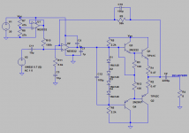
I'm unsure if C8 and C7 are correct, I mean, if that was what you were describing. C7 to me says, "super high f will see short and go straight to ground". C8 is a little unclear, but maybe, "super high f will see short to output, which will see short to ground".
The voltage regulated coming out of Q5 looks good to me, I need to do some math though and look in to why you chose 1k, 220, 47. 1k for ample bias current, right?
At V1 you can see L1, C1, C4, and C6. My thought process was, "low f sees L and will charge it and then pass through, high f will see open, but any that make it through will go straight to ground from that array of 10u, 1u, and 0.1u. Thoughts?
Output still looks good, I added the models for the MPSA56 and MPSA06. I had to switch the the alternate solver as the transient sims were gonna take an hour or so, and it seemed to work fine after that.
Attachments
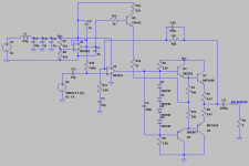
The collector of Q5 goes to the junction of R3 & R12. The bottom of R14 goes to negative rail, "ground". C7 & C8 are okay but you need another pair of capacitors from collector of Q5 to +29 and from collector of Q5 to minus rail "ground". 10 uf to 220 uf. This will make a center power supply for R3 & R12 to dump base current to.
I picked the resistor values out of the air. the current is lower out of the emitter of Q5 so that side doesn't need as much resistance as the collector. 250 + 47 ohms is 300 ohms, that would cause a 100 ma current, which gives a low enough impedance to dump base currents of Q3 & Q4 into without wobbling. A doorbell transformer is a 1.3 amp DC supply; presumably your wall plug switcher supply is even better than that. 100 ma of 1.3 amp is a negligable loss of power.
Some amps have the 220 ohm resistor between emitters of Q3 & Q4 and no capacitor, and there was a reason that didn't work as well as the two resistors to center voltage. I don't remember what it was but I think somebody said it was in Self's book.
I use too weird an operating system to run sims. Lubuntu14. But I never get viruses and it doesn't update when I first turn on the computer the way windows does. ^*#@_ Windows. I have a stupid phone too, not a smart one.
I may build one of these, I have a 29.5 v 2.5 amp supply and the LM1875 circuit is driving me nuts. IC circuit is too integrated to separate out where the problems are. Something (capacitor probably, maybe IC) is shorting on one channel causing motorboating, the other channel is dead although music from radio is getting to the IC minus input pin.
Last edited:
Trying to consolidate your advice. Is this what you're talking about? THD at 11%The collector of Q5 goes to the junction of R3 & R12. The bottom of R14 goes to negative rail, "ground". C7 & C8 are okay but you need another pair of capacitors from collector of Q5 to +29 and from collector of Q5 to minus rail "ground". 10 uf to 220 uf. This will make a center power supply for R3 & R12 to dump base current to.
I picked the resistor values out of the air. the current is lower out of the emitter of Q5 so that side doesn't need as much resistance as the collector. 250 + 47 ohms is 300 ohms, that would cause a 100 ma current, which gives a low enough impedance to dump base currents of Q3 & Q4 into without wobbling. A doorbell transformer is a 1.3 amp DC supply; presumably your wall plug switcher supply is even better than that. 100 ma of 1.3 amp is a negligable loss of power.
Some amps have the 220 ohm resistor between emitters of Q3 & Q4 and no capacitor, and there was a reason that didn't work as well as the two resistors to center voltage. I don't remember what it was but I think somebody said it was in Self's book.
I use too weird an operating system to run sims. Lubuntu14. But I never get viruses and it doesn't update when I first turn on the computer the way windows does. ^*#@_ Windows. I have a stupid phone too, not a smart one.
I may build one of these, I have a 29.5 v 2.5 amp supply and the LM1875 circuit is driving me nuts. IC circuit is too integrated to separate out where the problems are. Something (capacitor probably, maybe IC) is shorting on one channel causing motorboating, the other channel is dead although music from radio is getting to the IC minus input pin.
ALSO: Can I replace the 2222/2907s for 41C/42Cs? Or are they bad drivers?
Attachments
that THD is bad. try moving junction of 2 capacitors Vjunc to emitter of Q5. Sorry, that is the voltage stable point.
If THD doesn't improve, just build it with the original 200 ohm & 100 uf between emitters of Q3 Q4. But use a non-polar cap, there will be negative voltage on it at times.
If THD doesn't improve, just build it with the original 200 ohm & 100 uf between emitters of Q3 Q4. But use a non-polar cap, there will be negative voltage on it at times.
I couldn't figure it out. I moved back to the 220 ohm 100u configuration. THD down to 0.022181% (0.015590%). I'll make a BOM and post it here at some point.that THD is bad. try moving junction of 2 capacitors Vjunc to emitter of Q5. Sorry, that is the voltage stable point.
If THD doesn't improve, just build it with the original 200 ohm & 100 uf between emitters of Q3 Q4. But use a non-polar cap, there will be negative voltage on it at times.
Will also take a look at some heatsinks on digikey, maybe you can vet some of those I find. Also, under 1 amp, I can do this on a solder breadboard yeah? something like this
I build my DIP package projects on a board that looks a lot like that. The 5 holes should connect together horizontally. Center blank spacing should be 0.3" for DIPs. The boards I got from mcm had 4 holes in the corners for mounting, which I don't see on these. mcm was shut down, newark has them PN 21-4580 for $1.40 ea. https://www.newark.com/mcm/21-4580/medium-size-prototype-board/dp/25C3701 I use newark because they are closest to me in NC. NC is a long way from Oregon. Jameco in LA is close. My 3 hole version board allows me to connect two wires plus the dip socket together. I use sockets so I don't overheat the op amp IC with the iron.
You'll need a separate blank board for the big filter cap, the RF howl inductor, fuse holder, zobel network, etc. I mount boards to the metal case with #6-32 screws, elastic stop nuts, and 1/4 air tube cut up as spacers. If I was starting over I'd use 3 mm screws & nuts - weren't common until recently.
I like the TO220 heatsinks that have the fins bend forwards over the transistor body, instead of out to the side. The side ones make it difficult to cram two transistors together in a small board space. Takes #4-40 screws & stop nuts to go through a TO220 hole to heat sink, or maybe 3 mm (which I haven't tried since I have a whole can of 4-40) .
Last edited:
I think this is what you meant with the caps from rails to output? and also splitting the 220 ohm resistor. Also, what really pushed my response over was just changing the feedback cap to 100p, since that's my lowpass. 3dB point is at like 29k now.
All that time and trouble ....
Let me help - 12 cent junk drawer transistors = .001% THC ...
and happy listening. Below is my 10 year old amp.
Sim it , alter it ... whatever.
You would have to go much further to use a NE5532 as your IPS (also below) ,successfully.
PS - put the model .txt into the same folder with your simulation file (.asc)
click - go.
OS
Attachments
Some issues are:
1. Output transistors need to be BIG, and mounted on a BIG heat sink. The more you scrimp on them, the more grief you get when they die. Millions of amps have been built with marginal output transistors that work for a month or so and then die.
The rated power is usually specked for a case temperature of 25C. But no one has space for an infinite heat sink, so realistic power handling is scaled down by several factors. Most obvious is the thermal resistance of the heat sink and mounting pad, and transistor.
Then you have to decide how safe you want to be. Driving a capacitor, short or low impedance speaker can blow your transistors before you have a chance to correct the situation. Cut to the bottom line, don't expect more audio than about 1/4 the transistor power rating and be sure you have some kind of current limit. For an amp running +/-15V (30V total) you could get away with 50W transistors but better to go with TO220 or bigger, such as TIP-41 and TIP-42. Note that being "common" make these cheap, < $1.
2. Output swing. Your typical op-amp can not go closer than about 2V from the +/-15 rails, ie 13V peak, take away another 2V and we are down to about +/-11v, and your choice of which side to hang the bias makes that loss asymmetric. You can minimize it by bootstrapping "R17" so that it doesn't run out of current near the rail.
3. Novice mistakes include C2,C3 which are just going to charge up and cause cross-over distortion when driven or over-bias when not. You need to use smaller R5, R6 and carefully tweak R15, R16 for about 50mA idle current, less if Q5 is not mounted on the heat sink.
Also, D1, R1 is probably a bad idea, serves no useful purpose.
There are other things I could recommend but they would probably just get you in more trouble.
Post 24 was pretty good. Post 30 and 32 are bad ideas.
IC's are rarely used in professional designs because using ICs requires either more parts than no IC and/or serious performance compromises. IC's just have too much baggage. Some ICs do not have enough output current to make an amp with just two stages follower.
IC's are rarely used in professional designs because using ICs requires either more parts than no IC and/or serious performance compromises. IC's just have too much baggage. Some ICs do not have enough output current to make an amp with just two stages follower.
Attachments
Awesome, I will take a look at these when I have time this weekend.I build my DIP package projects on a board that looks a lot like that. The 5 holes should connect together horizontally. Center blank spacing should be 0.3" for DIPs. The boards I got from mcm had 4 holes in the corners for mounting, which I don't see on these. mcm was shut down, newark has them PN 21-4580 for $1.40 ea. https://www.newark.com/mcm/21-4580/medium-size-prototype-board/dp/25C3701 I use newark because they are closest to me in NC. NC is a long way from Oregon. Jameco in LA is close. My 3 hole version board allows me to connect two wires plus the dip socket together. I use sockets so I don't overheat the op amp IC with the iron.
You'll need a separate blank board for the big filter cap, the RF howl inductor, fuse holder, zobel network, etc. I mount boards to the metal case with #6-32 screws, elastic stop nuts, and 1/4 air tube cut up as spacers. If I was starting over I'd use 3 mm screws & nuts - weren't common until recently.
I like the TO220 heatsinks that have the fins bend forwards over the transistor body, instead of out to the side. The side ones make it difficult to cram two transistors together in a small board space. Takes #4-40 screws & stop nuts to go through a TO220 hole to heat sink, or maybe 3 mm (which I haven't tried since I have a whole can of 4-40) .
Are you saying I should hook up my source to the 4.7u into 1k with the 27k and 150p to ground after that? Maybe not to ground, but I need to take a longer look at what's going on here. This is your input stage correct? ill check it out in sim, thanks.All that time and trouble ....
Let me help - 12 cent junk drawer transistors = .001% THC ...
and happy listening. Below is my 10 year old amp.
Sim it , alter it ... whatever.
You would have to go much further to use a NE5532 as your IPS (also below) ,successfully.
PS - put the model .txt into the same folder with your simulation file (.asc)
click - go.
OS
Some issues are:
1. Output transistors need to be BIG, and mounted on a BIG heat sink. The more you scrimp on them, the more grief you get when they die. Millions of amps have been built with marginal output transistors that work for a month or so and then die.
The rated power is usually specked for a case temperature of 25C. But no one has space for an infinite heat sink, so realistic power handling is scaled down by several factors. Most obvious is the thermal resistance of the heat sink and mounting pad, and transistor.
Then you have to decide how safe you want to be. Driving a capacitor, short or low impedance speaker can blow your transistors before you have a chance to correct the situation. Cut to the bottom line, don't expect more audio than about 1/4 the transistor power rating and be sure you have some kind of current limit. For an amp running +/-15V (30V total) you could get away with 50W transistors but better to go with TO220 or bigger, such as TIP-41 and TIP-42. Note that being "common" make these cheap, < $1.
2. Output swing. Your typical op-amp can not go closer than about 2V from the +/-15 rails, ie 13V peak, take away another 2V and we are down to about +/-11v, and your choice of which side to hang the bias makes that loss asymmetric. You can minimize it by bootstrapping "R17" so that it doesn't run out of current near the rail.
3. Novice mistakes include C2,C3 which are just going to charge up and cause cross-over distortion when driven or over-bias when not. You need to use smaller R5, R6 and carefully tweak R15, R16 for about 50mA idle current, less if Q5 is not mounted on the heat sink.
Also, D1, R1 is probably a bad idea, serves no useful purpose.
There are other things I could recommend but they would probably just get you in more trouble.
Will take a look at this when I have some time, flooded with school right now. Thanks for all your input.Post 24 was pretty good. Post 30 and 32 are bad ideas.
IC's are rarely used in professional designs because using ICs requires either more parts than no IC and/or serious performance compromises. IC's just have too much baggage. Some ICs do not have enough output current to make an amp with just two stages follower.
EDIT: @steveu: do you recommend using the 41C/42C as drivers instead of the 2222/2907s?
Last edited:
Joe, I just received the transistors, thanks a bunch.I build my DIP package projects on a board that looks a lot like that. The 5 holes should connect together horizontally. Center blank spacing should be 0.3" for DIPs. The boards I got from mcm had 4 holes in the corners for mounting, which I don't see on these. mcm was shut down, newark has them PN 21-4580 for $1.40 ea. https://www.newark.com/mcm/21-4580/medium-size-prototype-board/dp/25C3701 I use newark because they are closest to me in NC. NC is a long way from Oregon. Jameco in LA is close. My 3 hole version board allows me to connect two wires plus the dip socket together. I use sockets so I don't overheat the op amp IC with the iron.
You'll need a separate blank board for the big filter cap, the RF howl inductor, fuse holder, zobel network, etc. I mount boards to the metal case with #6-32 screws, elastic stop nuts, and 1/4 air tube cut up as spacers. If I was starting over I'd use 3 mm screws & nuts - weren't common until recently.
I like the TO220 heatsinks that have the fins bend forwards over the transistor body, instead of out to the side. The side ones make it difficult to cram two transistors together in a small board space. Takes #4-40 screws & stop nuts to go through a TO220 hole to heat sink, or maybe 3 mm (which I haven't tried since I have a whole can of 4-40) .
I'm trying to finalize the design, but I'm running into some issues.
When I have drivers as 2222/2097s and outputs as 41C/42C, everything looks, mag response, transient, low-ish THD (1.01%).
But if I add either the MPS8099/MPSA55, OR MPSA06/56, in the simulation, my transient looks fine, but my mag response starts rolling off at like 10k, where instead I designed it to roll off around 29k.
I've been tinkering with it for a few days, and it seems that I can extend the mag response by designing R5/R6 (resistors above and below diodes) to rune more current down that branch. This makes sense to me: more current down this branch, more biasing current flowing to the output transistors, this turns them on and will operate into the higher frequencies better.
But, there's a tradeoff it seems. The lower I go with the resistor values, so more current down that branch, my output waveform starts railing super hard.
Intuitively, this makes sense to me, but I can't put my finger on what exactly is going on here. Am I running out of voltage headroom? Is it the LTSPice models that I'm using? What is a good standing Ic (dc dissipation) that I should be designing for to keep these transistors on in a good operation region? Currently, there's barely a uA running through the output transistor branch at DC.
Thanks for all your previous help.
- Status
- This old topic is closed. If you want to reopen this topic, contact a moderator using the "Report Post" button.
- Home
- Amplifiers
- Solid State
- DIY Amp Design Critique