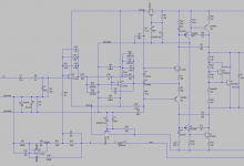
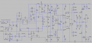
This amp frontend uses a dual op amp for its two input stages. It's driving a typical EF3 OPS with 30Mhz bipolar outputs, not shown.
The DC servo permits a wide range of op amps to work. Without the servo, the first op amp would have to be a JFET type.
Fast op amps in the signal path provide the cleanest gain and phase margins. They don't have to be fancy -- I've been simulating with the LT1253 "Dual low-cost video amplifier."
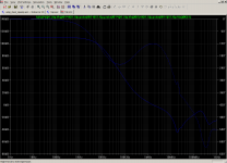
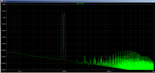
Each input stage has a pole and a zero. This yields "conditional stability" where the loopgain plot dips below -180db phase from the audio band up to ~200kHz, then recovers up to about -120db at the gain crossover point around 1.6MHz. We also get a whopping 80db of loopgain at 20kHz, pushing distortion performance deep past -100db. Spice shows distortion reaches -140db; that's probably optimistic.
Would a real build of this work? People get spooked about conditional stability. But it behaves nicely in the sim -- better than (say) CFP output stage designs I've abandoned because they couldn't handle fast squarewaves or clipping. This thing loves fast squarewaves. It clips okay.
You've got to ask yourself one question: do you feel lucky? Well do ya, punk?
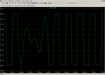
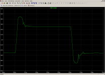
Attachments: loop gain plot, clipping behavior, 50kHz square wave (without the input RF filter cap), schematic, distortion spectrum.
The DC servo permits a wide range of op amps to work. Without the servo, the first op amp would have to be a JFET type.
Fast op amps in the signal path provide the cleanest gain and phase margins. They don't have to be fancy -- I've been simulating with the LT1253 "Dual low-cost video amplifier."
Each input stage has a pole and a zero. This yields "conditional stability" where the loopgain plot dips below -180db phase from the audio band up to ~200kHz, then recovers up to about -120db at the gain crossover point around 1.6MHz. We also get a whopping 80db of loopgain at 20kHz, pushing distortion performance deep past -100db. Spice shows distortion reaches -140db; that's probably optimistic.
Would a real build of this work? People get spooked about conditional stability. But it behaves nicely in the sim -- better than (say) CFP output stage designs I've abandoned because they couldn't handle fast squarewaves or clipping. This thing loves fast squarewaves. It clips okay.
You've got to ask yourself one question: do you feel lucky? Well do ya, punk?
Attachments: loop gain plot, clipping behavior, 50kHz square wave (without the input RF filter cap), schematic, distortion spectrum.
Attachments
Last edited:
Mouser has the LT1253. Nice DIP with legs. $5. The KSA parts I have my doubts. I managed to pry some KSA992 KSC1845 out of mouser but it took a 120 day backorder. They have some KSC1845 but never even heard of the KSA992 despite selling me some last year.
I think C23 the 2 pf cap is funny. 2 wires twisted together is 8 pf. Simulations!
So when are you going to build it?
I think C23 the 2 pf cap is funny. 2 wires twisted together is 8 pf. Simulations!
So when are you going to build it?
I think C23 the 2 pf cap is funny. 2 wires twisted together is 8 pf. Simulations!
What you really need is the equivalent to the finger that stops the oscillation with one connection.
")
Mouser has the LT1253. Nice DIP with legs. $5. The KSA parts I have my doubts. I managed to pry some KSA992 KSC1845 out of mouser but it took a 120 day backorder. They have some KSC1845 but never even heard of the KSA992 despite selling me some last year
I use KSC1845/KSA992, and I'm quite satified with them. Nice parts, to use instead of the discontinued 2SC2240/2SA970...
Sajti
For the 992/1845, any small high voltage bjts should work.Mouser has the LT1253. Nice DIP with legs. $5. The KSA parts I have my doubts. I managed to pry some KSA992 KSC1845 out of mouser but it took a 120 day backorder. They have some KSC1845 but never even heard of the KSA992 despite selling me some last year.
I think C23 the 2 pf cap is funny. 2 wires twisted together is 8 pf. Simulations!
So when are you going to build it?
The 2pF caps aren't critical, the circuit simulates okay without them. I put them in the schematic as a reminder to put pads for them in the layout, in case the opamps need to be tamed with a value in the 0-5pF range.
I'm with you about small value caps and how easily they can be swamped by parasitics. This circuit originally used NFB resistors of 56k and 2.2k. With those values the circuit worked best with a lead cap in the 1pF to 1.5pF range -- too small. Reducing the NFB resistors by 10x permits using a 10x larger lead cap for the same effect. At 10pF, maybe we can trust it.
What you really need is the equivalent to the finger that stops the oscillation with one connection.
I've been looking for one of these.
This amp frontend uses a dual op amp for its two input stages. It's driving a typical EF3 OPS with 30Mhz bipolar outputs, not shown.
Hi, what a good job!
1. Why Q9-Q11 uses common emitter? Common base is a way better.
2. Why two opamps for comparatively small gain? You can use uncompensated high-GBW ones like AD8067, LT1122, LM7171.
Opamp + Common base
3. Show your 3EF. Common mistake is not to stabilize it properly. There are at least two complicated ways.
4. Why so low ULGF?
It’s easy to design 6-7 MHz ULGF ~150dB/20kHz amp.
5. Why so much complicated correction?
Go inverting with two-three-pole compensation.
Last edited:
Hi BesPav,
1
1) Common emitter lets the output voltage get a little closer to the rail voltage. How is common base better? I'm seeing similar loopgain and similar distortion performance if I reconfigure it for common base.
2) Maybe this could be done with one opamp. Two gain stages makes it easy (lazy?) to design in two poles and two zeros.
4) I'm using 30MHz output devices. It seems aggressive to let ULGF go above maybe 2MHz with such devices...
5) It's not that complicated: each opamp stage has a LF pole, and a zero in the ~100kHz range. C11 and C12 create a third LF pole, this one has no zero to cancel it. The C6 lead cap adds some phase margin. Taken together, this shapes the loopgain for 80db of feedback at 20kHz.
What is two-three-pole compensation?
Common emitter lets the output voltage get a little closer to the rail voltage.
Yeah, but do you really came to rails and do you really limited in rail potential?
Anycase i’ll prefer to keep a good margin to rails due to strong nonlinear collector output capacitance vs collector-base voltage.
How is common base better?
It’s easy. CB influence nonlinearity due to Early effect while CE due to Early AND Miller effects.
I'm seeing similar loopgain and similar distortion performance if I reconfigure it for common base.
Now - yes.
You have loop’ed most of gain around two opamps and CE gain stage by C22, C23 and C11+C12.
While you need all your gain to restore High-frequency distortion of OPS you have looop’ed that gain around first stages.
Yes, you formed needed gain curve with proper margins, but there are a very suspicious dip at 20 MHz.
Where your high-voltage gain stage load? You have created very high resistance point between Q9-Q11 collectors, welcome to ultrasonic bath, keep your fingers out of the board and, of course, welcome to stability VS board manufacturing quality issues.
Maybe this could be done with one opamp. Two gain stages makes it easy (lazy?) to design in two poles and two zeros.
Yes, but loop all available gain around OPS, especially at high frequencies (30-300k) where “Solid state sounding” lives.
I'm using 30MHz output devices. It seems aggressive to let ULGF go above maybe 2MHz with such devices...
He-he.
No.
I know a very well sounding amp with 6-7 MHz ULGF based on 1,5-2 MHz output devices.
EF3 without special attention are unstable under load conditions. Do you really seen a flash with EF3 OPS self-destroying?
You need to make EF3 being EF2 at high frequencies 1-10M
There are two common ways.
First of - shut down first stage.
Last of - shut down last stage.
First will provide comparatively slow OPS, but could be very powerful.
Last could provide very fast OPS, but you need to keep second stage inside SOA.
It's not that complicated: each opamp stage has a LF pole, and a zero in the ~100kHz range. C11 and C12 create a third LF pole, this one has no zero to cancel it. The C6 lead cap adds some phase margin. Taken together, this shapes the loopgain for 80db of feedback at 20kHz.
Yes, clearly.
But really, this is not so good sounds as a designes.
Let’s talk about amp’s structure?
First block is a low-distortion differential line receiver with high CMRR, at least 70-90 dB around audioband.
Next will be volume regulation unit, of course, low-distortion.
And amp’s core will be only third.
Multiloop configuration are easy to design, but not so good in sounding. Try to loop as much as possible around OPS.
You picked proper HF opamps without very-low poles and obtain flat feedback depth, go further.
What is two-three-pole compensation?
Ok.
Fifth poles and two compensating zeros.


BesPav,
Thanks for the tips. I think this new schematic is more in line with what you are suggesting?
Here the FAST_NFB signal driving the lead cap is taken from predriver outputs at HF. At LF, the L-C filter keeps the whole output stage in the feedback loop. (TBD: can this be done without a choke?)
On the schematic, the op amps have moved inside a subblock representing a dual op amp -- this makes it easier to correlate the spice netlist with the PCB layout. For the same reason, the output transistors are omitted here; they're off the PCB. The outputs are 1302/3281 types.
I started with lighter compensation, where loop gain could go as high as 100db in-band with decent margins and -160db distortion performance. However square waves didn't do well at this level: under a large amplitude 50kHz square wave, the 1uF cap between the bases of the outputs tends to charge up a bit and overbias the output stage. The bias change moves the ULGF up too far, and HF oscillation begins. It's small amplitude, maybe it would be okay in practice.
Anyway I dialed the compensation back to 90db of in band loop gain and better stability margins all around. Square waves look perfect, distortion is -150db.
Attachments
Thanks for the tips.
Nothing for!
On the schematic, the op amps have moved inside a subblock representing a dual op amp
Ok, known gain with known poles/zeros are sufficient.
I think this new schematic is more in line with what you are suggesting?
Yes, better, but i'll prefer to exclude all Out_A and Out_B to B- and A- connections. Say, all your opamp block was make as crystal without external connections. Here are very old and very good article about external compensation:
http://www.ti.com/lit/an/slyt174/slyt174.pdf
Try to build an amp like figure 4 suggests.
Also pick this very practical Bruno Putzeys presentation:
http://www.diyclassd.com/img/upload/doc/an_wp/WP_AES123BP_the_engineers_survival_guide.pdf
Check slides from 13 to 48.
For the same reason, the output transistors are omitted here; they're off the PCB. The outputs are 1302/3281 types.
Let's start from the basics.
1. VAS.
Q9-Q11 collectors are better to load to something like 1 MOhm to ground, also pole could be placed there with very low NP0 capacitors. Keeping this point unloaded you have created very high resistance point (up to 100 Meg.). Nothing bad until real PCB will born in your fingertips.
2. OPS
Shown OPS will oscillate immediately after loading with any signal. Now this is much more Colpits generator than OPS.
There are common way to diagnose this. Disconnect all circuitry before OPS and keep only last VAS stage, bias and OPS. Provide proper bias by voltage sources to VAS. Load output by current source, say 1 Amp and draw output voltage vs frequency. Change scale to linear and you will see output impedance. If load are non unity amperes - divide to that value.
You will see some resonance peak around 5-30 MHz.
Your goal is to keep peak slopes inside second order rise and fall.
Do you need some images about?
There are two common ways to eliminate this issue.
1.a) Provide 150 Ohm base stoppers at Q15-Q16 bases between bias and OPS.
1.b)Provide 78-120 Ohm base stoppers at Q10-Q12 bases and add some capacitance between base and collectors of Q10-Q12, say 120-330pF.
1.c) Provide 3-5 Ohm base stoppers at bases of each output devices.
Doing this will exclude first stage of the OPS at high-frequencies and unstable EF3 becomes stable EF2
2.a) Also put that order base stoppers, but use even lower-frequency output devices, say MJL21193/94.
2.b) Change Driver devices to something higher-frequency'ed, say KSA1220A/KSC2690A. They not so good for driver load, but better 2SC4793/2SA1837 pair originals are obsolete as i know. One could let a try for any Toshiba licensiate, but check each device for Cob there are a lot of cheap fakes.
Doing this will also exclude one stage of the OPS, but now - last stage. At some MHz and tens of MHz driver devices will straightly work to load through huge Cbe of output devices.
The LG plot from post 11 may not be correct.
There are two global feedback loops here -- one defined by VOUT, the other by FAST_NFB. The FAST_NFB loop nests within the VOUT loop and excludes some of the output stage at HF.
Post 11 shows the LG measured within both loops. Here there are good stability margins.
If we move the probe to be within VOUT and outside of FAST_NFB, margins degrade, and 20kHz loopgain falls. This is not a highly stable amplifier. Experience with squarewaves suggests this, too.
- Status
- This old topic is closed. If you want to reopen this topic, contact a moderator using the "Report Post" button.
- Home
- Amplifiers
- Solid State
- Low distortion power amp frontend, done with opamps.