UgsQ5=Ur27+Ud3
That's right but that's ok. Otherwise, clipping begins a bit earlier for the bottom half-wave in quasi configuration. By the way clipping at the bottom is not as good and clean as at the top - this is something to think about in the future
")
P.S. Clipping with complementary OPS is very nice and clean.
All rubbish UD3 increase by Q5.That's right but that's ok. Otherwise, clipping begins a bit earlier for the bottom half-wave in quasi configuration. By the way clipping at the bottom is not as good and clean as at the top - this is something to think about in the future
P.S. Clipping with complementary OPS is very nice and clean.
All rubbish UD3 increase by Q5.
Well, the voltage gain of Q5 is close to 1 - what will amplify the rubbish are the output mosfets. However, the amount of rubbish with the diode and without the diode is practically the same - whatever happens in the negative rail, adds to Vbe of Q5.
Should resistors R17/19/21/23 be on mosfet Q5/7/9/11 sources instead on drains in quasi output stage? Top mosfets operate as common drain (gain less then 1), but lower ones operate as common source (with the gain more then 1) as they see speaker +drain resistors as load? Also, would putting resistors in sources instead of drains in lower half quasi OPS will give better current sharing between mosfets and better temperature compensation?
Should resistors R17/19/21/23 be on mosfet Q5/7/9/11 sources instead on drains in quasi output stage? Top mosfets operate as common drain (gain less then 1), but lower ones operate as common source (with the gain more then 1) as they see speaker +drain resistors as load? Also, would putting resistors in sources instead of drains in lower half quasi OPS will give better current sharing between mosfets and better temperature compensation?
Gosh!
Of course, they have to be on sources. Thank you for pointing this out.I have them on sources in the initial design and simulations, but then re-drawing the schematic in Diptrace with some copy/paste always leads to some stupid mistakes

Well, the voltage gain of Q5 is close to 1 - what will amplify the rubbish are the output mosfets. However, the amount of rubbish with the diode and without the diode is practically the same - whatever happens in the negative rail, adds to Vbe of Q5.
Ud3=U(j6)-Uc2. U(j6) do not constant.
Ud3=U(j6)-Uc2. U(j6) do not constant.
Uc2 is not constant either. We can consider a forward-biased diode being a voltage reference (a level shifter) in a wide range of currents.
As long as the "garbage" amplitude at j6 is not too high, it will be replicated at C2. Only if its amplitude will make D3 close at some positive peaks - then we have a certain difference of potentials at D3's ends.
In overall, you're right - it' will be better to move the diodes further "to the left" in this quasi design - putting them between the drivers and the VAS stage.
After all, unless I find a good solution for clipping in the negative half of the output signal, I consider the quasi option as an experimental one.
Cheers,
Valery
Could you try in sim whether adding "Baxandall diode" parallel to R26 in quasi output stage brings anything useful...the idea is to mimic the same paired V drop and impedance characteristic in the lower output half of the output stage as the paired base-emitter junctions occurring already in the top half.
Could you try in sim whether adding "Baxandall diode" parallel to R26 in quasi output stage brings anything useful...the idea is to mimic the same paired V drop and impedance characteristic in the lower output half of the output stage as the paired base-emitter junctions occurring already in the top half.
I have already performed some experiments - because of the HexFETs' rather high Vgs, I have to use something higher-voltage than a diode, but the idea is pretty much the same and it works well, also eliminating the "blip" when clipping. Please see the schematic in the next post.
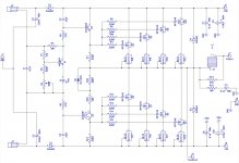
Updated Quazi OPS with lower distortion and good clipping
OK, now this one is good.
The network with zener at the driver's emitter leads to slightly lower distortion and much better clipping behavior. The bottom side clips a few volts earlier than the top one, but that's not an issue, considering there's no rail sticking or any other artifacts - clipping is flat now.
I will update the layout accordingly soon.
P.S. The OPS runs well at the quiescent current = 100mA per output pair. It can be raised up to, say, 300mA per pair for widening the class A region - just make sure to have some good heatsinks in this case - overall dissipation at 1.2A of the total idle current is not a joke anymore With +/-55V rails it comes to 130W per channel.
OK, now this one is good.
The network with zener at the driver's emitter leads to slightly lower distortion and much better clipping behavior. The bottom side clips a few volts earlier than the top one, but that's not an issue, considering there's no rail sticking or any other artifacts - clipping is flat now.
I will update the layout accordingly soon.
P.S. The OPS runs well at the quiescent current = 100mA per output pair. It can be raised up to, say, 300mA per pair for widening the class A region - just make sure to have some good heatsinks in this case - overall dissipation at 1.2A of the total idle current is not a joke anymore
With +/-55V rails it comes to 130W per channel.Attachments
Last edited:
...btw IRF540 is the same m-fet as IRFP240 in different housing.
Typing error...IRF640 is the same m-fet as IRFP240!
Could you try an IRF640 (without any suffix) wired as diode...btw IRF540 is the same m-fet as IRFP240 in different housing.
Good idea!
IRF640 with "gd" as an anode and "s" as a cathode works great.
Very slightly lower distortion at 1KHz, more significantly lower distortion at 20KHz. It has to be paralleled with 300R resistor for the best performance - this parallel combination provides the best "mimicking" of the top driver's characteristics.
It looks like my silly drawing error is leading to something good!
Jeff, you're right - many good things came to somebody's mind as a result of some kind of mistake
The layout with source resistors at the negative rail seems to me non-trivial though
Ok...caffeine is kicking: eek:
Let be clear about one thing…I'm not an EE...all the good things I've picked up in the last two decades come from a few geniuses in this forum and also to the geniuses they referred to ("the old guys"). So everything I say should be checked...at least twice
In input schematic split resistor R6 in two serial connected resistors (like 2*6k3 /2*6k8 or /2*7k5). Connect R5 top to newly midpoint between resistor (lets call them R6a-R6b). Now you have move your servo injection point completely from signal path. I predict you will be force lower R5 value to something like 10k or even less in order DC servo control to work properly.
Filter signal coming in and out from DC servo opamp...split R24 value in two and build RCRC input filter...do the same to opamp output signal...take 5k1 for R5/R7 value or something like that. As it is, servo opamp is wired as inverting integrator, should work…if not wire opamp as noninverting integrator
Loss C16 feedback cap...it may and probably will induce instability and/or oscillation...Compensation of an CFA should be done elsewhere.
Good idea!
IRF640 with "gd" as an anode and "s" as a cathode works great.
Very slightly lower distortion at 1KHz, more significantly lower distortion at 20KHz. It has to be paralleled with 300R resistor for the best performance - this parallel combination provides the best "mimicking" of the top driver's characteristics.
Good
...but for the best "mimicking" of the top driver's characteristics more radical surgery is needed...see LM12CLK simplified OPS for inspiration (this one comes from "old guys" at National Semiconductors)
Last edited:
Good
But that one is... complementary, no?
No it is not...it is the same quasi output stage found in all Overture series amplifiers like LM3886 and all sisters and brothers. That is the reason why every one is asking: "what that diode doing in the output stage"... it 'not an diode, it is npn transistor which behaves as diode at certain frequency.
- Status
- This old topic is closed. If you want to reopen this topic, contact a moderator using the "Report Post" button.
- Home
- Amplifiers
- Solid State
- Referenz - high-quality low-cost diy-friendly amplifier