Unsuspected stray capacitance can have a detrimental impact on the stability of the op amp.
See Figure 17. Comparison of output responses of the circuits in Figure 16.
The circuit at left resulted in the oscillatory response.
Practical Techniques to Avoid Instability Due to Capacitive Loading | Analog Devices
See Figure 17. Comparison of output responses of the circuits in Figure 16.
The circuit at left resulted in the oscillatory response.
Practical Techniques to Avoid Instability Due to Capacitive Loading | Analog Devices
Member
Joined 2009
Paid Member
when I design my pcb's I look at quite a few things -
I use wide & short traces where possible to reduce inductance and resistance, also to improve heat flow away from the solder joints and related components. It's quite important around through-hole pads if you are going to be repairing boards or changing out parts so I use large pads where I can.
I try to run traces in pairs, since current flows in loops I like to have the current return path follow back adjacent or underneath the outgoing current. In other words, low loop-area reduces radiation and magnetic coupling.
I try to keep high impedance sensitive nodes away from areas with large voltages and potential noise to reduce capacitive coupling.
I don't like having power supply connections on opposite sides of the pcb, I want to bring twisted wires into one side only. Same for other signals.
Lastly, and no less important, the layout should look nice, it should have some beauty of it's own. You can often tell when somebody used autoroute because the layout is not at all aesthetically pleasing. Don't ask why this is important - you either have a feel for this or you don't.
Last edited:
I like your list, Bigun.
I'd just add one thing: when you can't keep sensitive traces completely away from dirty ones, at least run them at right angles to each other.
Here's an example from a preamp:
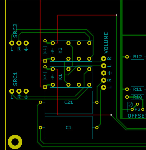
K1 and K2 are relays that select the input. Their 12V power lines come in on the front of the board (red traces). Note how they are not optimized to be short, but rather to stay away from the input traces (on the back of the board, in green) until they have to cross, and then to do so at right angles.
I'd just add one thing: when you can't keep sensitive traces completely away from dirty ones, at least run them at right angles to each other.
Here's an example from a preamp:
K1 and K2 are relays that select the input. Their 12V power lines come in on the front of the board (red traces). Note how they are not optimized to be short, but rather to stay away from the input traces (on the back of the board, in green) until they have to cross, and then to do so at right angles.
Attachments
Last edited:
Piglet'sDad over on PinkFishMedia mentioned that the NAP250's regulator was greatly compromised by having its VAS referenced to the noisy power rails (thereby giving it poor PSRR at high frequencies -- right where the NAP amp circuit needs it).
So I tried a version with the VAS referenced to ground (which also means flipping the LTP):
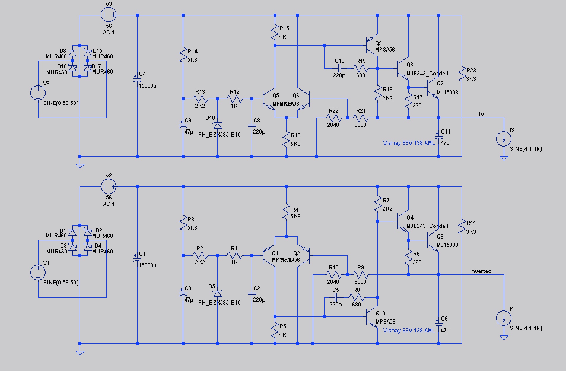
(This also has the advantage of looking like a VAS followed by a Darlington, rather than visually masquerading as an output triple.)
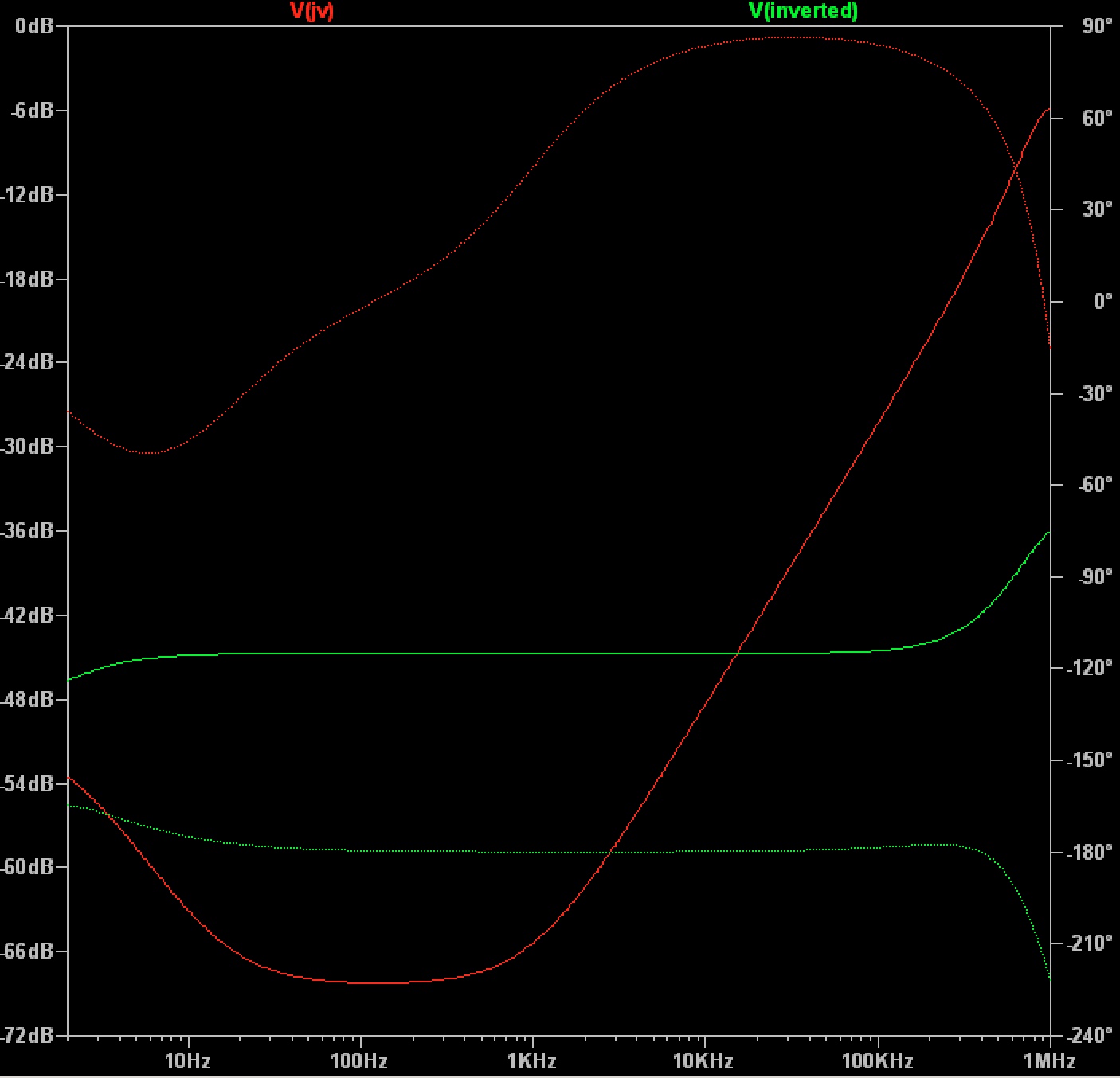
While it has vastly improved attenuation at high frequencies, it gives it back a low frequencies:
Swapping a resistor for a JFET lets us have our cake and eat it too:

So I tried a version with the VAS referenced to ground (which also means flipping the LTP):
(This also has the advantage of looking like a VAS followed by a Darlington, rather than visually masquerading as an output triple.)
While it has vastly improved attenuation at high frequencies, it gives it back a low frequencies:
Swapping a resistor for a JFET lets us have our cake and eat it too:
Attachments
Naim NAP regulator (sans current protection):
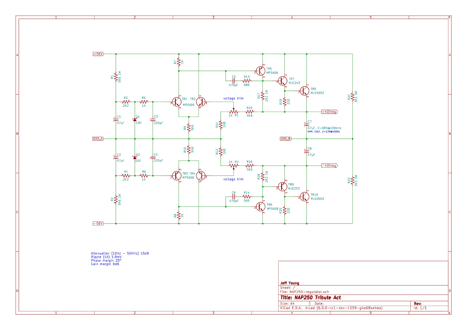
Modified regulator. LTP & VAS re-referenced to ground, CCS added for LTP, Miller compensation changed from local to global.
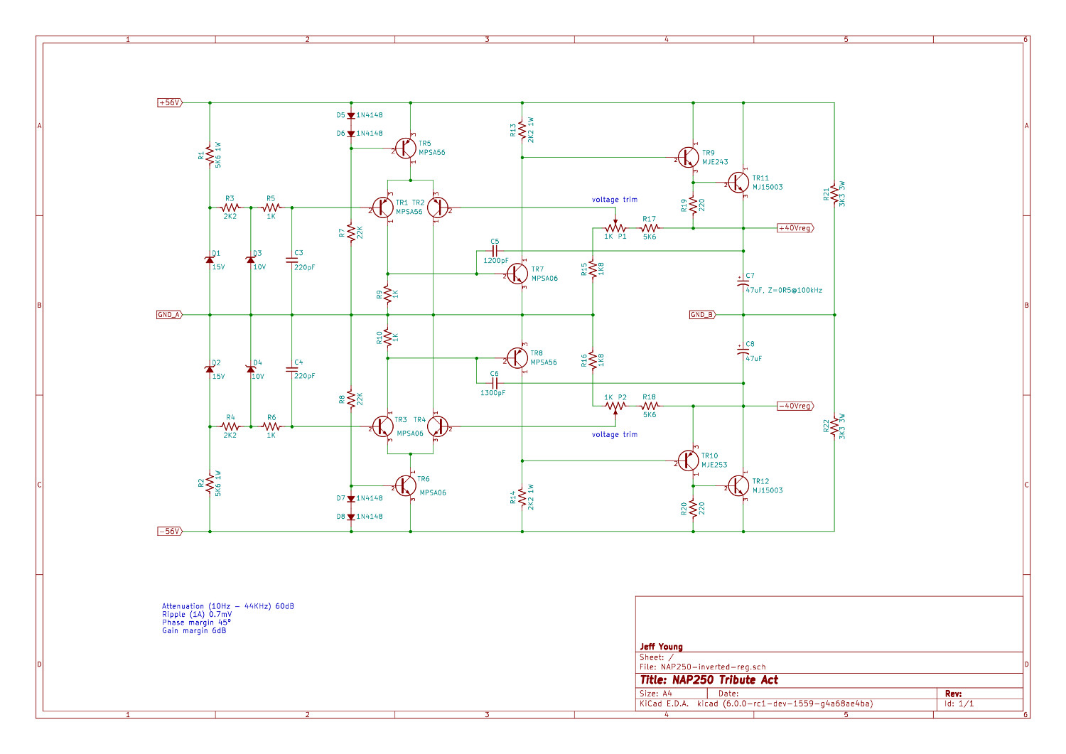
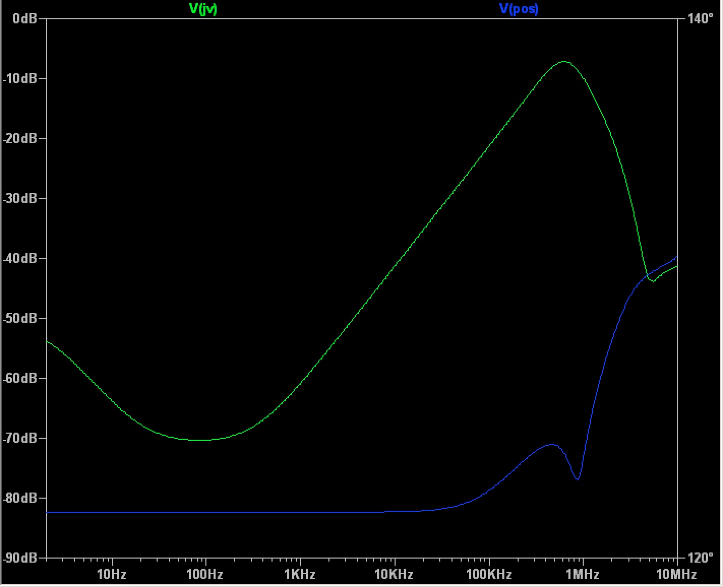
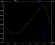
SPICE has the modified regulator giving vastly better performance in the higher frequencies:
Can you hear the difference? Dunno. But I intend to find out.
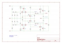
Naim schematic board:
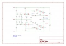
Modified schematic board:
Modified regulator. LTP & VAS re-referenced to ground, CCS added for LTP, Miller compensation changed from local to global.
SPICE has the modified regulator giving vastly better performance in the higher frequencies:
Can you hear the difference? Dunno. But I intend to find out.
Naim schematic board:
Modified schematic board:
Attachments
The traces between the Miller cap and the VAS transistor on the amp board are about as short as they can get.
So let's assume you're talking about the regulator boards. Naim's design has a resistor in the Miller circuit, so it is what it is. Those traces could be shorter though. How's this:
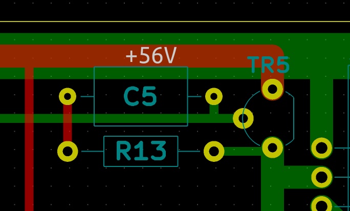
On the modified regulator the Miller cap is bypassing the VAS & the output stage. There's no way to make that particularly short.
I'm not trying to be dense; I just am.")
So let's assume you're talking about the regulator boards. Naim's design has a resistor in the Miller circuit, so it is what it is. Those traces could be shorter though. How's this:
On the modified regulator the Miller cap is bypassing the VAS & the output stage. There's no way to make that particularly short.
I'm not trying to be dense; I just am.
Attachments
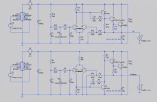
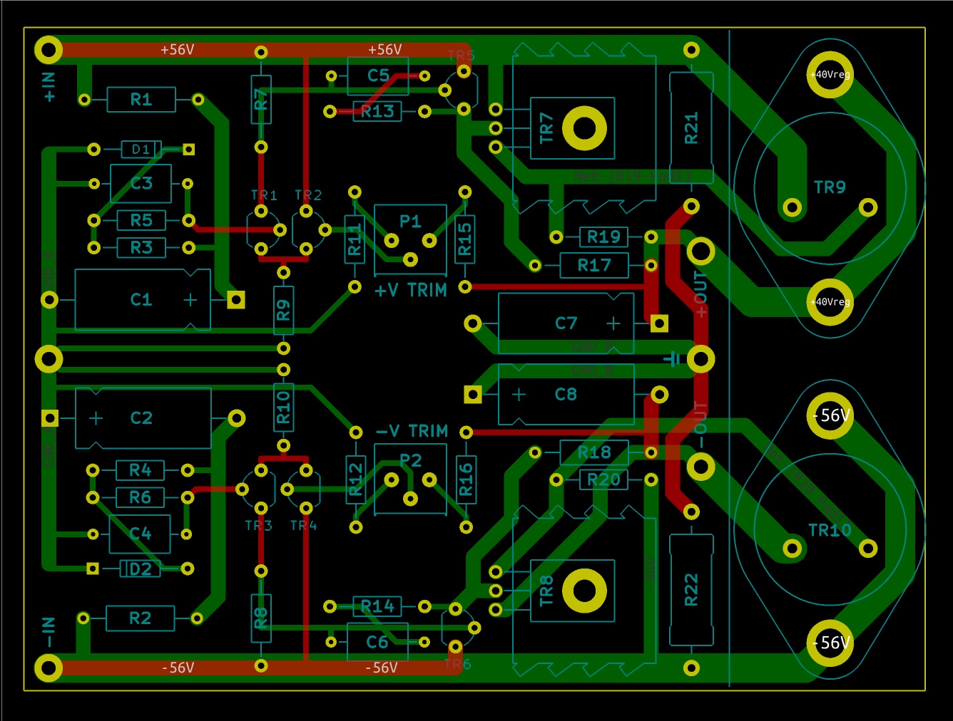
I did manage to find some styrene 39p caps for the amp boards. They're chunky little buggers, though, and will make the traces a bit longer. Go with them or the mica's and shorter traces?
An externally hosted image should be here but it was not working when we last tested it.
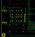
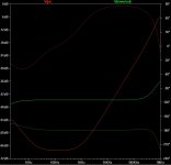
Even my first layout was reasonably compact next to Julian Vereker's.
VAS in red, Miller cap & resistor in blue, and traces connecting them in green.

Granted, he had the constraints of a single-layer board. But I don't think Naim amps come with radio licenses, do they?
VAS in red, Miller cap & resistor in blue, and traces connecting them in green.
Granted, he had the constraints of a single-layer board. But I don't think Naim amps come with radio licenses, do they?
Attachments
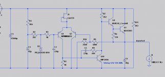
A cm or two is ok. But your second regulator schematic (post #67) will be unstable. Even if the simulation doesn't show it.
Last edited:
Second regulator schematic from post #67 is the global feedback one.
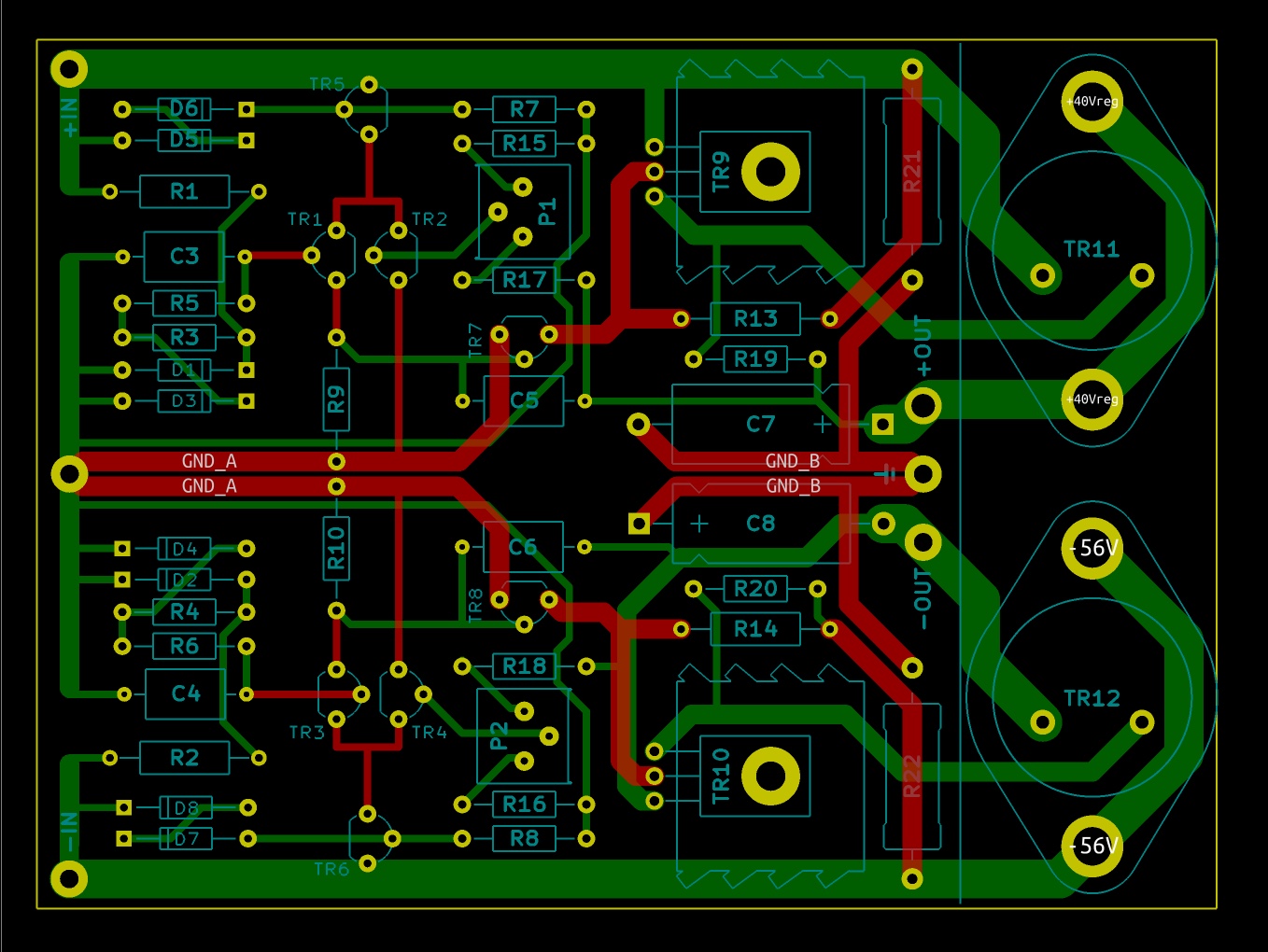
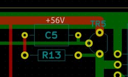
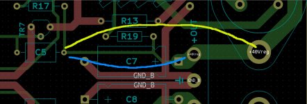
What's the operable length? Just to the current-carrying trace (blue line), or all the way to the output device (yellow line)?
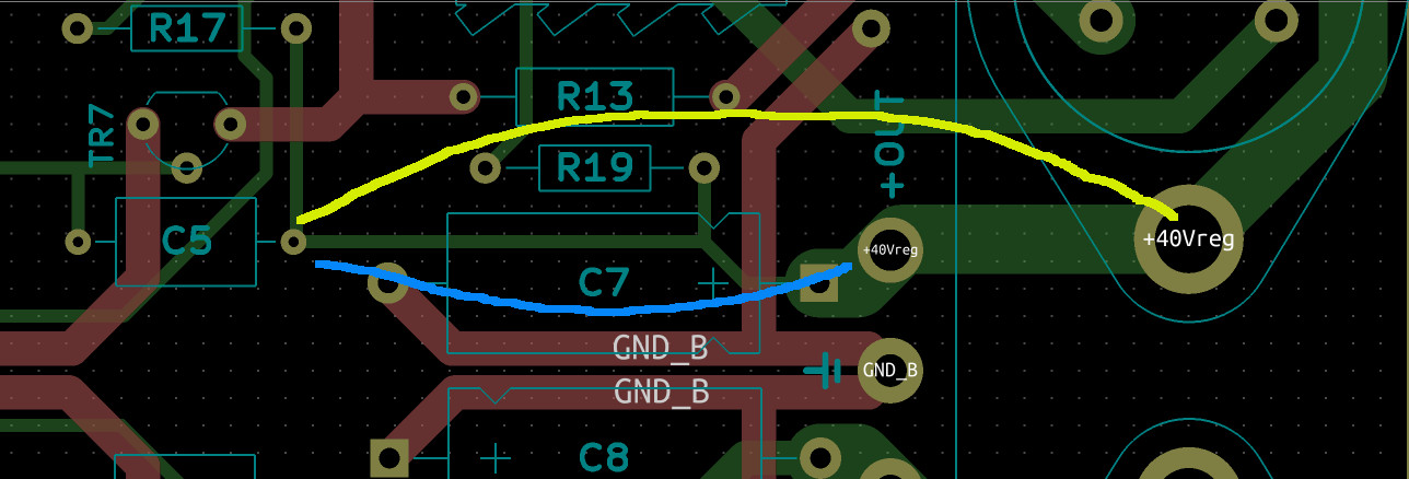
And what's the problem with the length? The trace resistance shouldn't matter: it will just add a zero (which in fact would be mildly useful up at about 47R, but that would be a really long trace).
Is it ringing? C7 is connected in the middle and is an electrolytic so it will have a non-trivial ESR even at high frequencies. Wouldn't that dampen any ringing?
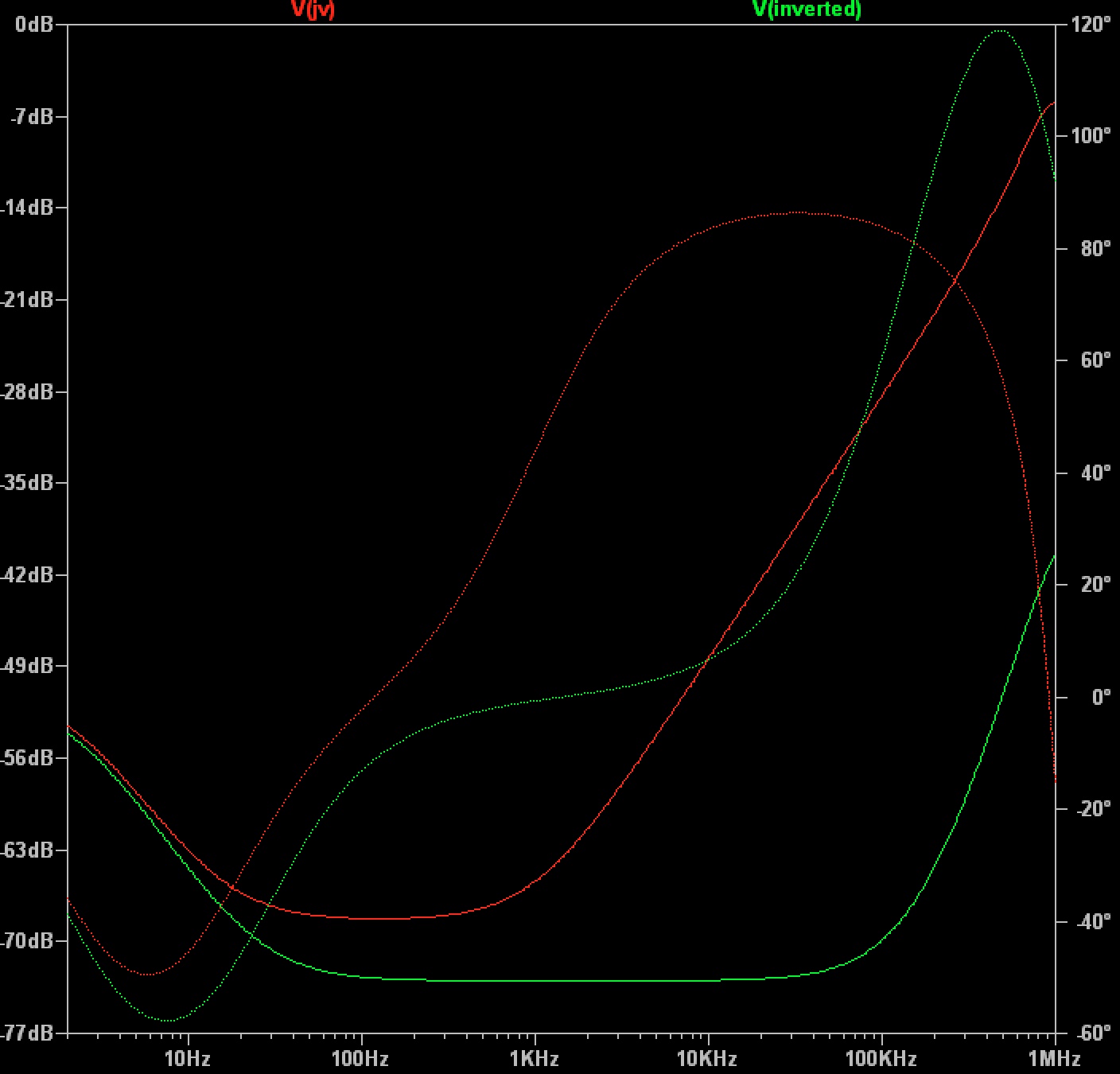
Is it the trace inductance? The yellow length will have an inductance on the order of 50nH. If I plug that into SPICE I do get an ugly spike at 50MHz. Shortening the trace to about 1cm moves that out to 100MHz. But 1cm doesn't even get me out from under the heat-sink.
The 50MHz spike is around -35dB, while the 100MHz one is around -40dB. Those are waaay below unity gain.
What am I missing?
What's the operable length? Just to the current-carrying trace (blue line), or all the way to the output device (yellow line)?
And what's the problem with the length? The trace resistance shouldn't matter: it will just add a zero (which in fact would be mildly useful up at about 47R, but that would be a really long trace).
Is it ringing? C7 is connected in the middle and is an electrolytic so it will have a non-trivial ESR even at high frequencies. Wouldn't that dampen any ringing?
Is it the trace inductance? The yellow length will have an inductance on the order of 50nH. If I plug that into SPICE I do get an ugly spike at 50MHz. Shortening the trace to about 1cm moves that out to 100MHz. But 1cm doesn't even get me out from under the heat-sink.
The 50MHz spike is around -35dB, while the 100MHz one is around -40dB. Those are waaay below unity gain.
What am I missing?
Attachments
Well...I hesitate to start down the “advanced electronics course” route. And giving all the answers might kill your DIY entertainment. If you don’t mind spending on having different PCBs made then maybe you should try them and see. The best thing I can recommend is prototyping on a breadboard. Then you can try many arrangements and see what you get.
What test equipment have you got?
What test equipment have you got?
I did digital hardware (professionally) back in the 1980s, but then moved into software.
Since retirement I've built a tube amp (a Bottlehead SEX with some changes to the PSU), a hybrid headphone amp (my version of a TorpedoIII) and a couple of Pass amplifiers (F3 and F5). The SEX is a point-to-point, but all the others are on my own PCBs.
I got the HP from AccuSource in GA some years ago.
To the point, two parallel wires have about 3 pf per cm of capacitance to each other. That couples high frequency signals of the two inputs . Any sharp vertical voltage changes have large high frequency components. As rectifier shutoff, for example.And what's the problem with the length? The trace resistance shouldn't matter: it will just add a zero (which in fact would be mildly useful up at about 47R, but that would be a really long trace).
Is it ringing?
What am I missing?
Building on PCB's IMHO maximizes this effect, because of long parallel traces. In 3D as I build, wires in space don't couple so well because they are farther apart, and rarely parallel.
If you have an actual noisy run, try putting pads at each end and run a loopy wire up in the air. This coupling effect won't show up in sims.
Last edited:
If C1, C3 & C4 are tantalums they need to be high voltage, like 25V or more. This is to do with making sure they have enough reverse voltage tolerance.
Unfortunately, this is incorrect.
Vishay, for example, does not give any guideline but simply advises that tantalum capacitors are never used in a circuit where a reverse voltage may be applied across its terminals. This is good advice.
For those that do the common guidelines for reverse voltage are:
10% of rated voltage to a maximum of 1 volt at 25°C
3% of rated voltage to a maximum of 0.5 volts at 85°C
1% of rated voltage to a maximum of 0.1 volts at 125°C
So for reverse voltage considerations only, there is no advantage to increasing the rated voltage above 10V if you believe that the cap will not get hotter than 25°C - which is pretty optimistic even with a Class B Naim amp.
VishayUnfortunately, this is incorrect.
Vishay, for example, does not give any guideline but simply advises that tantalum capacitors are never used in a circuit where a reverse voltage may be applied across its terminals. This is good advice.
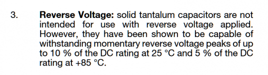
See guidelines section 3.
Source?For those that do the common guidelines for reverse voltage are:
10% of rated voltage to a maximum of 1 volt at 25°C
3% of rated voltage to a maximum of 0.5 volts at 85°C
1% of rated voltage to a maximum of 0.1 volts at 125°C
Attachments
- Home
- Amplifiers
- Solid State
- NAP250 clone