I am building my first 1969 PA from scratch. Instead of using 2N3055, I select MJL3281AG from ON as the output transistors. Before building the Amp, I simulate the circuit by means of Multisim 14.0.
Due to the lack of basic knowledge, I am not able to figure out the functionalities of every R and C in the circuit. Therefore, in order to minimize the THD (measured by Multisim), I adjust the R and C again and again. However, this is definitely not a good solution.
I post here to hope if anyone could tell me the functionalities of the circuit. Here is my circuit.
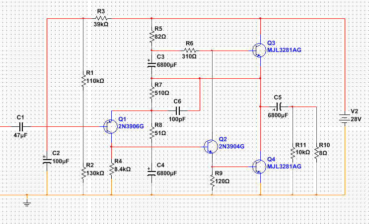
(see attachment if the image is broken.)
Let me explain the modifications:
1. Change to 2N3906/2N3904/MJL3281AG because they are in production.
2. Change C4 and C5 to larger one to extend low audio frequency.
3. Change C3 to larger one because larger one seems to give lower THD measured in Multisim, expecially in low audio frequency range.
4. Change input capacitor C1 to larger one for Bode compensate introduced by large C4 and C5.
5. Add C6 to avoid high frequency instability.
6. Change almost every R base on THD measurement .
.
My concern is:
1. 2N3904 is 650 mW max. Using 2N3904 is not safe here (now, P = 300 mW). However, changing 2N3904 to other NPN parts gives some larger THD. (now is 0.01%, after changing, it increases to 0.03% @ 1kHz) Any advice?
2. Feedback resistor R7 and R8 is much smaller than that in the original design (2.7k and 220 respectively). Changing to larger R7 and R8 (while keeping their relative value) gives larger THD, but why?
3. R5 and R6 are small resistors in value. Are they thermal stable. How about the Q-point stability?
4. R9 is changed to small 120 (original is 2.2k) to lower the static current passing through MJL3281AG. But is it still thermal stable? I don't know its functionality.
5. Any bad effect when changing C1, C3 and C4 to larger one? One of the bad effect is C4 need more time to charge and discharge.
My final goal is to build 1969 using parts in production.
I really appreciate your help!
Best,
Guan
Due to the lack of basic knowledge, I am not able to figure out the functionalities of every R and C in the circuit. Therefore, in order to minimize the THD (measured by Multisim), I adjust the R and C again and again. However, this is definitely not a good solution.
I post here to hope if anyone could tell me the functionalities of the circuit. Here is my circuit.
(see attachment if the image is broken.)
Let me explain the modifications:
1. Change to 2N3906/2N3904/MJL3281AG because they are in production.
2. Change C4 and C5 to larger one to extend low audio frequency.
3. Change C3 to larger one because larger one seems to give lower THD measured in Multisim, expecially in low audio frequency range.
4. Change input capacitor C1 to larger one for Bode compensate introduced by large C4 and C5.
5. Add C6 to avoid high frequency instability.
6. Change almost every R base on THD measurement
.My concern is:
1. 2N3904 is 650 mW max. Using 2N3904 is not safe here (now, P = 300 mW). However, changing 2N3904 to other NPN parts gives some larger THD. (now is 0.01%, after changing, it increases to 0.03% @ 1kHz) Any advice?
2. Feedback resistor R7 and R8 is much smaller than that in the original design (2.7k and 220 respectively). Changing to larger R7 and R8 (while keeping their relative value) gives larger THD, but why?
3. R5 and R6 are small resistors in value. Are they thermal stable. How about the Q-point stability?
4. R9 is changed to small 120 (original is 2.2k) to lower the static current passing through MJL3281AG. But is it still thermal stable? I don't know its functionality.
5. Any bad effect when changing C1, C3 and C4 to larger one? One of the bad effect is C4 need more time to charge and discharge.
My final goal is to build 1969 using parts in production.
I really appreciate your help!
Best,
Guan
Attachments
Last edited:
PNP sanken A1216 JLH1969 single-ended class A power amp kit 10W+10W L168-27 | eBay
This makes things easy...buy the kit, assemble it, mod it, enjoy it
Use proper power supply and heat sink.
This makes things easy...buy the kit, assemble it, mod it, enjoy it
Use proper power supply and heat sink.
I thought the 2n3904 was a bit underspecced for the signal splitter transistor. It needs to be able to drive the output transistors which requires a bit of current. My JLH 96 uses a BD139 here, on a heatsink.
If you read the original JLH article from 1969, if I recall there is a table of certain resistor values to set quiescent current depending on your speaker impedance, probably not wise to change those.
Why don't you just look at the 96 JLH circuit for transistor numbers, and build the original JLH 69 with those modern transistors? Or just build the '96?
I am perplexed by the sanken A1216 kit from e-bay. JLH himself explained in one of his books that output transistors should be slow, not fast as Sankens are. Stability of the circuit depends on it. The fastest transistors to be used are MJL 2119x, at 4MHz. MJL3281 are not transistors for this circuit.
Hi ivanlukic,i have test the JLH 10W and the bigger version using TTC5200 and i can't see any instability no at the fft analyzer not on the scope.I am perplexed by the sanken A1216 kit from e-bay. JLH himself explained in one of his books that output transistors should be slow, not fast as Sankens are. Stability of the circuit depends on it. The fastest transistors to be used are MJL 2119x, at 4MHz. MJL3281 are not transistors for this circuit.
apparently it works even with fast MOSFETS, and it sounds good too...
J554 P-MOS FET JLH1969 Class A Power amplifier kit (2 channel amp kit) | eBay
J554 P-MOS FET JLH1969 Class A Power amplifier kit (2 channel amp kit) | eBay
You might be better off moving this to the much bigger JLH Class-A thread....more likely to meet the hard core 10 watt fans.
Also its worth reading the Geoff Moss Class-A amp site now being hosted by Elliot Sound Products in Sydney. There is a lot of material there that saves a lot of time and energy.
Cheers Jonathan
Also its worth reading the Geoff Moss Class-A amp site now being hosted by Elliot Sound Products in Sydney. There is a lot of material there that saves a lot of time and energy.
Cheers Jonathan
Last edited:
You might be better off moving this to the much bigger JLH Class-A thread....more likely to meet the hard core 10 watt fans.
Also its worth reading the Geoff Moss Class-A amp site now being hosted by Elliot Sound Products in Sydney. There is a lot of material there that saves a lot of time and energy.
Cheers Jonathan
Thank you, Jonathan! I will try to discuss here. Yes, save a lot of time and energy.
Best,
Guan
PNP sanken A1216 JLH1969 single-ended class A power amp kit 10W+10W L168-27 | eBay
This makes things easy...buy the kit, assemble it, mod it, enjoy it
Use proper power supply and heat sink.
Thank you, adason! It is really a better choice to buy a KIT, I think.
Thank you, adason! It is really a better choice to buy a KIT, I think.
No need to buy a kit with fake parts.
Prasi's pcb is excellent and you can buy original parts to be sure for results
JLH 10 Watt class A amplifier
Last edited:
Should not the mid point of R1 and R2 be connected to the base of Q1??
The idea is that the emitter of Q1 should be around half supply voltage for max output and min THD.
Without it there is no bias for Q1 and anything can happen, in sim and real-life....
R11 is superfluous and only wastes a (little bit of) power.
Jan
The idea is that the emitter of Q1 should be around half supply voltage for max output and min THD.
Without it there is no bias for Q1 and anything can happen, in sim and real-life....
R11 is superfluous and only wastes a (little bit of) power.
Jan
Last edited:
Should not the mid point of R1 and R2 be connected to the base of Q1??
The idea is that the emitter of Q1 should be around half supply voltage for max output and min THD.
Without it there is no bias for Q1 and anything can happen, in sim and real-life....
R11 is superfluous and only wastes a (little bit of) power.
Jan
Yes, it is connected to base of Q1 (screenshot don't show the cross point, sorry). How about R4/R7/R8 and R9?
Guan
Why have you changed the values of R7 and R8 (your references) away from the design values?
R7 sets the available current for Q1 and is a critical component. It was 2k7 in the original as I recall.
Yes, it is 2k7 in original design. I change them because I find a decreased in THD in Multisim.
Have a look at the stability at HF with those changed values. It may well be a little worse.
Thank you. I now know that R4 and R7 together control Q1's Q-point. You are great!
I found JLH comment on his own 1969 amp. You are right that Sankens and fast ONSemis can be used. He says that speed of Q1 and Q2 should be much lower than speed of Q3 and Q4 so that the circuit "has an in-built dominant lag in it's loop NFB characteristics. This ensures that the loop gain has fallen below unity before the loop phase angle reaches 180 degrees. No additional HF compensation networks are therefore necessary to ensure complete loop stability, even with reactive loads".
Just be sure that input transistors are much faster than output transistors.
Just be sure that input transistors are much faster than output transistors.
- Home
- Amplifiers
- Solid State
- JLH 1969 Explanation