Hi all.
Need collective intelligence, since I am out of ideas.
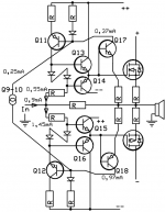
n900 mosfet poweramp goes to protection because of 5V DC at the output and unstable biasing. Pre-driver output cut, power stage input shunted 5k to ground. Got -12V at the output and very wierd voltages across Q211 and Q212 (see picture). All Q211-Q218 checked good, D230/231 and D233/234 are also good, D227 replaced to semitec 1ma CRD, D226 was good but replaced, D224 good, output mosfets checked good.
another working amp in same config with cut predriver shows 0.5v DC at the output.

Need collective intelligence, since I am out of ideas.
n900 mosfet poweramp goes to protection because of 5V DC at the output and unstable biasing. Pre-driver output cut, power stage input shunted 5k to ground. Got -12V at the output and very wierd voltages across Q211 and Q212 (see picture). All Q211-Q218 checked good, D230/231 and D233/234 are also good, D227 replaced to semitec 1ma CRD, D226 was good but replaced, D224 good, output mosfets checked good.
another working amp in same config with cut predriver shows 0.5v DC at the output.
Perhaps something wrong with Q217 or the resistors around it.upd: 120k resistor ground to base of Q211 does the thing. But Q209 and Q210 also checked good...
Mona
Have you checked all voltages from regulators first?
sure, voltages are fine
Perhaps something wrong with Q217 or the resistors around it.
Mona
I just removed Q217. No effect.
You said a resistor of 120k to gnd solved the problem.I just removed Q217. No effect.
It is that transistor that provide a current at the same place, probably missing.Can be the transistor or one of the resistors or the base-drive with problems.
Mona
You said a resistor of 120k to gnd solved the problem.
It is that transistor that provide a current at the same place, probably missing.Can be the transistor or one of the resistors or the base-drive with problems.
Mona
Mona, thanks for your involvement. Still stuck.Put all transistors back, got +4v at TP2. Checked everything, just don't know what to do. What if I disconnect output stage from power rails (they are feed from separate PSU)? Should the whole section with Q209-Q218 be stable - I understand this is not an amplifier, just "distortion correction" circuit?
Q208, Q209, Q211 and Q212 are for the bias current.
Q213, Q214, Q215 and Q216 are the drivers.
Q217 and Q218 give a little positive feedback for the drivers, don't now why.
The others are for current limiting of the output.
Left alone, connection to the pre-amp cut, the output at TP2 is never realy zero, the feedback to the input has to correct that.
That is, your 5k to gnd doesn't give the final stage the input to correct it's DC-shift.
Mona
Well, OK. With input cut and 5k to the ground, no rails voltage at the power mosfets stage - should TP2 being stable (with some DC)? Because now I have its raising from +5 to +15VDC and goes back to +5VDC every 2 second. D203 and D212 are also cut, just to exclude any influence of protection circuit as well as c213/c214.
A voltage going up and down every 2seconds looks like some oscillation.
How, i don't no.Perhaps via the positive feedback Q217,Q218 but to have such a slow variation normally is with big capacitors, missing here.
And at the start of this threat you had minus 12V ??
I don't see where those big ups and downs come from.
Mona
How, i don't no.Perhaps via the positive feedback Q217,Q218 but to have such a slow variation normally is with big capacitors, missing here.
And at the start of this threat you had minus 12V ??
I don't see where those big ups and downs come from.
Mona
yes, it seems like oscillation but with no caps its weird. Oscillation at TP2 starts with +3v raising up to +18 within 35-40 secs, then it drops sharply back to +4v and starts to sway with 2 secs period.
I had -12v without q217/218, but once putting them back I got +4v at once. Then cut power rails on mosfets - get oscillation. The oscillation itself is also strange - the voltage across the bases of Q211 and Q212 is constant 147v, but if each base measured to the ground - its sways 65v to 79v.
So my point is to simplify circuit as much as possible, just to retain very few parts and get it 100% works as it should. Then to start adding other parts and see on which point it starts faulting.
Since it's an interesting problem, i studied the thing a little closer.
Q17 and Q18 are adjusting the current at the final stage input according to the (miss match) of the Pmosfet Vgs and the Nmosfet.The difference causes the driver to deliver a current to get zero volts.
So probably a or several mosfets gate-source voltages misbehave.
The hole final is no more then a symetrical source follower, no reason to oscillate.
Mona
Attachments
")
Well, it seems I possibly found the reason. After removing all Q213-Q218, there's only biasing circuit remains Q209-Q212. After checking there is strong and stable -5 volt at the R344/R234 joint. But there should no be, physically - no source for any voltage there. I have removed them both along with jumper wire connecting it to the mosfets. Voltage remains - very surprising. Very. Cleaned the pcb and surrounds, top and bottom. Still there. Then figured R224 goes just above this PCB route (crossing), so parasite induction was a suspect. I raised R224 for 2mm above the board and yes, -5V goes to zero, as it should be. Now putting everything back for testing...

Nice if you found a solution !
But i can't follow your expication.Are the numbers on the PCB different from the schematic ?
You say after the removing of the resistors the problem isn't gone but by puting them back somewhat higher helps ??
Mona
I try to clarify:
1. I have removed R233 and R234: voltage -5V was still on the PCB route.
2. Then I raised R224 by 2mm above the board - problem has gone.
So apparently R224 (TKD brand, wirewound) was inducing some very minor current to the PCB route it is crossing. Occasionally, the point, where such induced current was found, was directly connected to the mosfets gates. So I just increase the distance between R224 and the board.
- Status
- This old topic is closed. If you want to reopen this topic, contact a moderator using the "Report Post" button.
- Home
- Amplifiers
- Solid State
- Stuck again with Sony mosfet repair