...Also keep in mind you need an adequate power supply, better LLC...
Did you study the power supply in post #27?
Looks better than LLC but I haven't done sims yet.
But, really, before you continue, check this:
https://www.audioxpress.com/files/attachment/2659
I didn't know about that one until your previous link to it, probably the way of the future but where is the fun to just buy an IC?
")
Best wishes
David
...It has occurred to me to use some kind of self oscillation control loop on a buck converter power supply.
Seems this could solve the control problem of how to maintain Zero Volt Transitions as the load varies.
There are a few patents for this but I haven't had time to study them carefully.
...
I studied US4857822A - Zero-voltage-switched multi-resonant converters including the buck and forward type
- Google Patents and now understand the problem better.
The variation in load doesn't necessarily mess up the ZVT but does result in increased back EMF on the switch MOSFET.
For a simple quasi-resonant circuit the stress on the FET increases in proportion to the load variation.
For an audio amp with 200 mA quiescent and 20 A peaks (600 W "RMS" into a <4 ohm subwoofer) that means 100x multiplication of the ~100 V supply.
Obviously not acceptable and I can't see how the control loop can fix this, so must have some kind of clamp.
Now I understand why there are so-called "Active Clamp" buck converters.
Anyone experienced with this?
David
For a simple quasi-resonant circuit the stress on the FET increases in proportion to the load variation...
Perhaps this problem is why quasi-resonant and multi-resonant circuits are still somewhat niche.
I had an idea to use a saturable inductor in the quasi-resonant circuit that sets up the ZVT.
Then if the load current increases the inductance drops and the inductive back EMF stays fairly constant.
Unlike the clamped circuit, this is fairly novel AFAIK.
Anyone seen this?
(Finally, a question where a lack of responses will be a compliment, implies it may be a new idea
)...Only output mosfet power supply...float... I don't see the stray capacitance problem.
No, probably not a problem for you.
This is a monoblock or stereo amp and the floated supply(s) will be small, separate transformer(s)?
Mine is a home theatre system so that a separate floated supply for each channel means a lot of extra supplies.
I would like to make amp boards that could just drop in to replace a standard amp.
So they need to run on the usual, simple DC power.
I could have another small on-board DC-DC converter to create the floated supply but that adds complexity of course.
Best wishes
David
Last edited:
Perhaps this problem is why quasi-resonant and multi-resonant circuits are still somewhat niche.
I had an idea to use a saturable inductor in the quasi-resonant circuit that sets up the ZVT.
Then if the load current increases the inductance drops and the inductive back EMF stays fairly constant.
Unlike the clamped circuit, this is fairly novel AFAIK.
Anyone seen this?
(Finally, a question where a lack of responses will be a compliment, implies it may be a new idea
No, probably not a problem for you.
This is a monoblock or stereo amp and the floated supply(s) will be small, separate transformer(s)?
Mine is a home theatre system so that a separate floated supply for each channel means a lot of extra supplies.
I would like to make amp boards that could just drop in to replace a standard amp.
So they need to run on the usual, simple DC power.
I could have another small on-board DC-DC converter to create the floated supply but that adds complexity of course.
Best wishes
David
Hi David,
Yes, I am using separate low voltage transformer and that is cumbersome to implement.
I was trying to find isolated drop down buck converters from 60V to 6 to 7V 10 to 15A but could not find. In this case I would use LLC SMPS +-60V to drive everything except low voltage output transistors driven with drop down buck converters. I don't see at this moment anything better than ClassD to modulate low voltage stage power supply, it does not need to be very low distortion.
Best wishes, Damir
...I don't see..better than ClassD to modulate...power supply...
Hi Damir
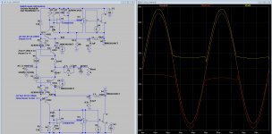
I have come up with this.
It looks simple but all the hard work was to make it as simple as possible.
Efficiency looks excellent, only a few watts at quiescent and linear up to the first watt too.
Then the rail trackers switch on - and it hits 600 W into 4 ohms easy.
All with ridiculously low distortion because the output transistors have a very stable Vce.
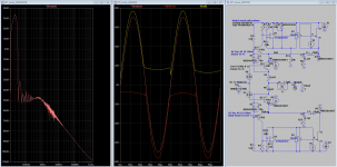
The simulation has 3rd harmonic down >75 dB @ 20 kHz into 8 ohms, and that's with no feedback at all, just a skeleton of output transistors.
Second picture shows 8 ohm FFT and 4 ohm @ 600 W .Tran simulation.
Add -ve feedback from the amp and the lower limit should be...set by how perfect the layout and PCB details rather than the schematic.
I have left a few critical details hidden on the schematic but it's basically accurate.
I will send you the full ASC if you are interested.
I think it's time I start to build this.
Best wishes
David
Attachments
Last edited:
Sorry my DIYaudio PM box is full but I sent the ASC to your .Gmail.
Best wishes
David
Received, thanks
Damir
I want to consolidate in this thread some email discussions with friends who have the complete ASC.
Hopefully others may have some ideas or information.
"We don't need the special GaN transistors, it would be simpler to use silicon FETs.
Then we could use complementary P and N and avoid hi side driver and power supply complications.
The output would be essentially identical, the cost would be more power dissipation rather than any waveform difference.
The GaN FETs claim to be quite robust, the Safe Operational Area is better than many MOSFETs.
There seems to be no second breakdown or the MOSFET equivalent, not sure if it's true.
I am inclined to do a prototype with silicon, maybe do the GaN FETs as version 2."
GaN FETs do seem to be practically immune to the second breakdown type behaviour of low Ron silicon FETs.
They do have very small thermal mass, potentially a problem that low frequency may thermally cycle the transistors into premature failure.
"The several MHz operation looks like a problem.
But GaN Systems claim their LTspice model is validated.and the GaN FETs are supposed to be able to handle it.
And as you noticed, their power dissipation is quite low.
Reality will set in on the transition rise and fall rate rather than the pulse frequency itself.
This should be controllable with Gate resistors, perhaps separate rise and fall resistors.
As you say, PCB layout will be critical, for both EMI and just to make it work,
...
So I have started on a PCB layout, just pencil and paper at this point.
I will probably learn KiCad once I have some ideas pinned down.
It seems it could work on an Insulated Metal Substrate board if the substrate was used as a Ground plane.
I could find no examples of this to study details, IMS is usually used one sided with slow LEDs."
Anyone know about hi speed use of IMS?
David
Last edited:
I’ve done a fair bit of microwave stuff on IMS. LNAs, mixers, strip line filters etc.
Most of the microwave board stock makers (Rogers etc) do their substrates with thick copper (1/4”) as an option. It’s handy for doing all sorts of things.
This is all single-sided though, with the backing metal as a ground plane. We generally didn’t do it for thermals, but mainly just to get a really good ground plane.
Big advantage of working with this stuff is you can mount SMA strip line launchers right on the board.
I wouldn’t use the stuff for audio though, as it’s very hard to work with. You really need a mill to cut out your cavities and make ground connections, plus work with a temperature controlled hot plate when you’re attaching surface mount devices.
I’ve done a fair bit of microwave stuff on IMS...
Most of the microwave board stock makers...do their substrates with thick copper (1/4”)
..it’s very hard to work with. You really need a mill to cut out your cavities and make ground connections...
Hi Suzy, nice to have comments from someone with actual experience.
All I have so far is the idea that it should work well.
It would combine the really solid plane for hi frequency EMI control, with nice thermal performance.
I do have a mill so that's no problem, and Toni "ASTX" has one with CNC.
So we can cut tracks as well as cavities.
How do you do your ground connections?
Some PCB makers talk of "HDI" or "stacked" vias.
I would like to know more about the details of this, a different process to the usual drilled and plated vias.
But probably we will just drill or mill down to the copper, as I expect you do.
Do you really use 1/4" copper, 6.35 mm?
Did you mean 1.6 mm perhaps?
Best wishes
David
Last edited:
No, definitely 1/4 inch, or 6mm. You need that thickness because a lot of microwave parts (splitters, amplifiers, mixers) came in “flat pack” packages, which were a lot like modern smd parts but with straight pins on 0.1” centres, in hermetic metal cans. You mill a cavity for the parts, etch the top layer into the pattern you want, then drop some solder paste into the cavity for the amplifier ground, which is made between the back of the part and the bottom of the cavity.
When we needed to bring ground to the top of the board we’d drill a hole, squirt some solder paste in, and press a teeny little rivet into the hole. The top of the rivet was flared, so would make a good connection with the trace.
All the reflow was done on a hot plate, so you’d put paste on, mount all the parts and rivets, then pop the assembly on a hot plate to reflow.
It’s remarkably hard to find pictures.
These are the sort of packages:
P2-03-301 - Pulsar Microwave | Power Divider
These are the sort of packages:
P2-03-301 - Pulsar Microwave | Power Divider
No, definitely 1/4 inch, or 6mm....
That is remarkable, the skin depth of copper at hi frequency is only a few micrometres or less so it seems very wasteful to use a thick, heavy, not inexpensive slab of it.
And pure copper is a pain to mill, which makes it even less understandable.
Use an alloy to make it easier to mill and you lose most or all of the conductivity improvement over, say aluminium.
When was this? I expect it's hard to find pictures because it is not done much anymore?
The tiny rivets you mention were basically what I had in mind, I just planned to drill thru the PCB then insert tinned copper wire and snip it to size before I solder, thanks for that.
You have any experience with the fast transitions of GaN transistors?
At the moment it's a toss-up between that and complementary silicon FETs.
The GaN looks quite robust but would require a floated supply
Probably use an isolated DC-DC converter across the lo V rails, adds maybe $20-$30 dollars.
You have any comments on the schematic itself?
Best wishes
David
GAN is tricky, tricky stuff, VERY fast transitions and the difference between fully conducting and blown out the gate is way too close.
It is telling that most GAN seems to have an explicitly separate source connection far the driver because you just cannot get the loop area down for enough any other way.
I have played with it in an envelope tracking transmitter (Kind of similar to your audio doings), and it does work but I needed at least two layers on a metal core board, and blew up a lot of transistors.
Also, you will really, really need a seriously quick scope and maybe a rogowski probe or such to try to see what it is that is eating your fets at random times (Usually a source/gate transient about 100ps long, trick is catching the bugger).
Looking at your circuit, whatever devices you use (I would go for Si, there is no need for anything that fast in an audio amp), you will want a diode in series with the base of each of the two outer bipolars as otherwise when the thing winds toward the opposite rail you will seriously reverse bias the base emitter junction, and they are usually only good to a few volts.
An interesting thought is to either remove the inner rail entirely, (Allow the collector of the inner devices to sit a few volts above or below the emitter all the way to the opposite rail, VERY nice for SOA with reactive loads, but the switching frequency will vary widely), or to set the inner rail to zero volts (Not quite as nice for SOA, but somewhat more conventional).
GAN is tricky, tricky stuff, VERY fast transitions...most GAN seems to have an explicitly separate source connection far the driver
I can always slow down the transitions with driver output resistors of course.
That partly defeats the point of GaN, but easier to slow down a fast transistor than try to speed up a slow one.
The transistor I used in the sim is a GaN Systems GS61008 which does not have a separate "Kelvin" source connection.
They address this point in the datasheet, claim it is not necessary.
https://gansystems.com/wp-content/uploads/2020/04/GS61008T-DS-Rev-200402.pdf
But, yes, it worries me.
I have played with it in an envelope track[er]...(Kind of similar...), and it does work but I needed at least two layers on a metal core board, and blew up a lot of transistors.
The similarity had already inspired me to look at such envelope trackers to see what I could learn.
Nice to read your practical experience - about what I expected, more blown transistors than I hoped.
Also, you will really, really need a seriously quick scope...
Yes, this is the problem - My scope is too slow and a seriously quick scope is seriously expensive.
What did you use?
I don't work at this stuff professionally so I don't have a well equipped employer's lab that I can use after hours.
This may be the deal breaker.
whatever devices you use...you will want a diode in series with the base of each of the two outer bipolars...
...is to either remove the inner rail entirely, (Allow the collector of the inner devices to sit a few volts above or below the emitter all the way to the opposite rail, VERY nice for SOA with reactive loads...or to set the inner rail to zero volts (Not quite as nice for SOA, but somewhat more conventional).
And thank you for the specific ideas re the circuit, I will have a closer look at the simulation and see what I can.
I had the idea that the circuit but without the switch mode components could still be a nice Class H amp, just less efficient and therefore lower output power before thermal limit.
Maybe make the switch mode Class H for the sub woofer and woofer and just simple Class H for the mid horn lower power requirement.
That would make the GaN FETs overkill, fast silicon would be more than adequate for subs and woofer use.
Simplifies life and makes the whole system cheaper.
I think that's the way I will prototype.
Best wishes
David
Last edited:
In that application the copper is mainly a heat spreader, RF power devices tend to run at the outer limits of what is possible power density wise, and soldering the device package down to a big solid piece of copper makes the subsequent thermal interface to the heatsink run at far lower power density.That is remarkable, the skin depth of copper at hi frequency is only a few micrometres or less so it seems very wasteful to use a thick, heavy, not inexpensive slab of it.
David
In cost constrained usage you sometimes see a copper 'coin' fitted into a hole in a mostly conventional board and then over plated, but that is only really cost effective at scale as it makes the PCB processing non standard, while a copper IMC is a standard process.
Dave, any chance you could send me the .asc I want to have a play?
I am thinking that making both rails track all the way might be interesting (Loose the inner rail and connect the switcher diodes to the opposite rail instead of ground, sort of idea).
+-80V rails, two pairs of transistors for the class AB bit with about 5V or so across each, simple current limit at maybe 20A, and a P/N channel mosfet or so to do the switching? Most expensive part will be the high saturation current inductors, Wurth have something that looks sane, but it is not cheap.
In that application the copper is mainly a heat spreader, RF power devices tend to run at the outer limits of what is possible power density wise...
A copper IMS makes perfect sense, it's just that that I have never seen 6 mm copper IMS.
At that thickness I would have expected to use aluminium, maybe copper or silver plated, much easier and faster to mill, and cheaper.
But if 6 mm is indeed available then my horizons are broadened, so much the better
Dave, any chance you could send me the .asc I want to have a play?
...Loose the inner rail and connect the switcher diodes to the opposite rail...
+-80V rails, two pairs of transistors for the class AB bit with about 5V or so across each, simple current limit at maybe 20A, and a P/N channel mosfet or so...
I am very happy to send you the ASC.
Send me an email so I know your address, mine is in my DIYaudio profile.
Your proposal is not so far from my current candidate.
Outer rails at 80 V for 600 W nominal power output into 4 ohms, yes.
The output transistors I use work a little better at +-10 than 5, and the SMPS has an auxiliary supply of +-12 V, so maybe a bit more than 5 but it's a minor detail.
Complementary Mosfet for simplicity, yes.
The switcher rail connection had not occurred to me, exactly the kind of fresh idea I hoped someone would contribute.
Not sure how it will work but very interested to see what you have in mind.
You were, of course, correct about the need to protect the outer transistors from excessive reverse Vbe.
I haven't updated the ASC yet.
Best wishes
David
Last edited:
- Status
- This old topic is closed. If you want to reopen this topic, contact a moderator using the "Report Post" button.
- Home
- Amplifiers
- Solid State
- Very Efficient Very Low Distortion Linear+ Amp