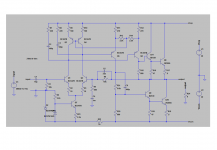
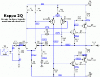
This circuit is inspired on two background ideas. One is from John Linsley-Hood's ClassA 10W design, and later modifications; the other is from Mullard's 10-15W Class A circuit which was published in the second edition of their Transistor Audio and Radio circuits, which showed a differential driver to a Darlington output and driver pair for each output half.
The similarities are slight. This design uses a more modern approach, with a differential input stage, a high impedance transistor pair which sets the current in the differential driver-VAS combination and a driver-output transistor pair.
The quiescent current in the prototype was set by choosing component values after measuring the gains of the output and driver transistors. I happen to have obtained high gain 2N3055's from ON Semi, so as this is a development circuit, it may be that other devices will need adjustment. The easiest approach would be to use a pot in the CCS of the input stage.
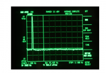
Simulated distortion was 0.002% at 1kHz.
I measured the prototype with a bias current of 1.5A and supply rails of 20V at just before clipping (which turned out to be due to the PSU with a hard clamp at 2A; will repeat with capacitor filters) at 0.005%. Circuit is shown with distortion image.
Temperature stability of the bias current is a question, but because the driver stage is set by the Vbe's of Q3, Q4 then as the unit warms up the current will actually drop, so essentially safe. But there will be a signifcant change as the transistors warm up. These are mounted on a 0.5K/W heatsink, but so far the current has not shifted too much.
More info as I get the results later.
The similarities are slight. This design uses a more modern approach, with a differential input stage, a high impedance transistor pair which sets the current in the differential driver-VAS combination and a driver-output transistor pair.
The quiescent current in the prototype was set by choosing component values after measuring the gains of the output and driver transistors. I happen to have obtained high gain 2N3055's from ON Semi, so as this is a development circuit, it may be that other devices will need adjustment. The easiest approach would be to use a pot in the CCS of the input stage.
Simulated distortion was 0.002% at 1kHz.
I measured the prototype with a bias current of 1.5A and supply rails of 20V at just before clipping (which turned out to be due to the PSU with a hard clamp at 2A; will repeat with capacitor filters) at 0.005%. Circuit is shown with distortion image.
Temperature stability of the bias current is a question, but because the driver stage is set by the Vbe's of Q3, Q4 then as the unit warms up the current will actually drop, so essentially safe. But there will be a signifcant change as the transistors warm up. These are mounted on a 0.5K/W heatsink, but so far the current has not shifted too much.
More info as I get the results later.
Attachments
Member
Joined 2009
Paid Member
Member
Joined 2009
Paid Member
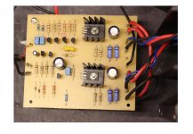
Here is a picture of the dev. PCB. It's a neat layout approx 80x100mm.
Possible updates for a PCB design would be to add a pot. for bias current control as mentioned, proper terminals (not good old pins) and transistor connections for e.g. TIP3055 rather than TO-3 which need the flying leads.
Some points on the design:
one of the limitations in JLH's original Class A design was that the output transistors could only change base currents where the increase in one device was obtained by reducing the current in the other. To be able to increase the base current further, a driver transistor is required so that more current can be obtained if needed. Secondly, the drive current available needs to be increased.
As pointed out on the JLH10 thread, thermal stability was assured by the fact that the driver current was limited, despite looking dubious.
In this design, the higher current available does lead to a potential thermal issue, but there are two mitigating features. First, emitter resistors are used, which helps. Secondly, the current drive is derived from the emitter-base voltages of Q3 and Q4, and as they reduce with temperature, the current drive reduces too. The ratio of R15:R12 (or R20:R11) is such that 2.5 times the voltage change is applied. That is intended to compensate the driver and output transistors with global temperature.
The emitter resistors and large heatsink control the current during the initial warm-up period. With a pot, the current can be set after warming up rather than at switch-on if that is important.
The differential VAS stage is fed differentially from the input pair, one side driving each output and driver stage. Q3 and Q4 work as a sort of "dual current mirror" except they common mode out the combined current from the VAS stage.
One guide to the success of this -still relatively simple - design is that the current swing in the output transistors has reduced from (simulated) 20% distortion (internal currents) in JLH's original 10W to 10% i.e. the current swings are more linear. Partly the emitter resistors will apply local feedback, which helps.
If anyone is interested in a PCB perhaps a revised design can be generated. If arranged for TIP3055's then also perhaps MJL21194's or even MJL3281A's could be used. A first simulation suggested that the distortion could go below 0.001% with those.
Attachments
That is quite elegant - very good prototype performance from comparatively few & v low-tech parts. I like it!
Might a large-ish decoupling cap be worth adding across D2? 100uF or more? It could help bolt-down the PSRR for the LTP, since D2 will have a min few-tens to- c.100 ohm impedance vs R22? (I suggest it, only because at these rail voltages it's a very cheap measure; and I cannot see it could do any harm!)
Might a large-ish decoupling cap be worth adding across D2? 100uF or more? It could help bolt-down the PSRR for the LTP, since D2 will have a min few-tens to- c.100 ohm impedance vs R22? (I suggest it, only because at these rail voltages it's a very cheap measure; and I cannot see it could do any harm!)
Martin
You raise an interesting point.
One of the key points about this design is its symmetry. Any signal entering the CCS should affect both sides equally and therefore the output would not see this. That is just CMRR.
So I simulated a PSU signal injected in series with the 1k resistor (not the negative power rail). There was a 1.4uV peak to peak output for a 1V disturbance. But I noted that, in common with many capacitor coupled/decoupled signals, the differential drifted with each pulse. It follows that because the two sides to the differential input stage are unbalanced, this was the prime cause. I have never seen anyone balance the input and feedback capacitor before, but adding a 680 ohm in series with the input capacitor, and changing this to 1mF the two sides are identical. The simulation then showed less than 0.1uV ripple which was absolutely flat, showing that CMRR can be effective when properly balanced.
However adding a 330uF capacitor across the first Zener (D2, which is 10V if the diagram is not clear) even this reduced to almost nothing.
Unfortunately when the signal is applied to the power rail rather than the input stage, the output signal was about 90uV. That says the output stages are the biggest contributor to (degraded) PSU rejection. Therefore, a power supply filter would have better impact than a relatively cheap capacitor, as many found with the original JLH. Though I agree the capacitor improves the situation and could be included in a future revision.
Last edited:
The more I look at this design the more impressed I am with it - either that or I am not understanding fully the benefits of this topology - several things I don't remember seeing before.
I've seen that current mirror trick in Cordell's amplifier, he explains in some thread how it works.
Well, not according to simulations. The concept is to provide a collector voltage variation which produces an Early effect distortion to counteract the Early effect distortion on the right hand side.A resistor in that position does not reduce distortion, on the contrary, it does much damage (along with the current mirror). I am expecting very low bandwidth and high distortion from the BD139-2N3055 compound @ 1.5 A.
The low bandwidth might be true if it were not for the 100pF capacitor across the resistor. In addition the local base and emitter resistors provide some local feedback.
Note that the impedance the BD139 base sees is 680 ohms, not 5.6k.
As for the current mirror "damaging" the performance, maybe you could say how.
On the contrary, it keeps the currents in the differential driver stage constant, and provides a very high impedance to both sides so that even with 270 ohm emitter resistors the OLG is high. I would agree that the 100pF capacitors roll off the gain but the frequency at which this begins is in the high audio end, so has little effect on the performance.
ALso the 2N3055's I used are modern epi base with fT's of about 3MHz. Measured fhfe is 60kHz (on previous samples) which is well above audio, so no bandwidth limit there, but as mentioned the circuit also seems to have lower distortion with high ft transistors. Mainly, I suggest, through the linear gain performance.
Last edited:
Martin
You raise an interesting point.
One of the key points about this design is its symmetry. Any signal entering the CCS should affect both sides equally and therefore the output would not see this. That is just CMRR.
So I simulated a PSU signal injected in series with the 1k resistor (not the negative power rail). There was a 1.4uV peak to peak output for a 1V disturbance. But I noted that, in common with many capacitor coupled/decoupled signals, the differential drifted with each pulse. It follows that because the two sides to the differential input stage are unbalanced, this was the prime cause. I have never seen anyone balance the input and feedback capacitor before, but adding a 680 ohm in series with the input capacitor, and changing this to 1mF the two sides are identical. The simulation then showed less than 0.1uV ripple which was absolutely flat, showing that CMRR can be effective when properly balanced.
However adding a 330uF capacitor across the first Zener (D2, which is 10V if the diagram is not clear) even this reduced to almost nothing.
Unfortunately when the signal is applied to the power rail rather than the input stage, the output signal was about 90uV. That says the output stages are the biggest contributor to (degraded) PSU rejection. Therefore, a power supply filter would have better impact than a relatively cheap capacitor, as many found with the original JLH. Though I agree the capacitor improves the situation and could be included in a future revision.
Thanks for the detailed response; interesting analysis.
I'd only observe that adding-in your 330uF cap is cheaper / more-robust than requiring to specify a maximum preamp output impedance, to ensure this effect on balance - i.e. requiring a preamp broadband output z a small percentage of that 680ohms value critical to peak CMRR; or 20pence worth of capacitor?
Next stupid suggestion - and a wild one this - what effect might replacing Q8-Q11 with a pair of mosfets have? Not because I am a particular fan, but you have - presently c 2.1v bias at the VAS output, easily adjusted to suit; and so likely headroom to use an source resistor for each if it would help O/P bias stability; and the effective unloading of the differential VAS might be interesting in the light of your findings to date (the second stage will really only then see gate charge/discharge currents, which might help reinforce the balance condition from LTP into differential VAS.)
I freely confess - this is just a 'whatabout-ism' not considered in detail: my apologies if a useless distraction.
Last edited:
Trev - yes, that is the idea. I wanted to see what feedback there might be on this circuit to incorporate or adapt it if anyone has constructive suggestions. My changes so far are to incorporate a trim pot for the output current; the 330uF capacitor across the Zener and possibly arrange for TO-218/TO-264 devices instead of TO-3 to simplify wiring.
Hi,
I see no affinity with the JLH amplifier that has single-ended predrivers and this is a Japanese style fully balanced circuit. What is the role of R21?
To me it looks kinda like Elvee’s Circlophone. Transistor polarities are swapped, which is why it took a couple of days to sink in. He used a zener in place of R21 to soak up the extra voltage. Low dynamic resistance and helps keep the thermals the same in the driver pair.
- Status
- This old topic is closed. If you want to reopen this topic, contact a moderator using the "Report Post" button.
- Home
- Amplifiers
- Solid State
- 16W Class A - inspired by JLH